P89V662FBC,557 NXP Semiconductors, P89V662FBC,557 Datasheet - Page 49
P89V662FBC,557
Manufacturer Part Number
P89V662FBC,557
Description
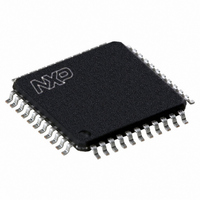
IC 80C51 MCU FLASH 32K 44-TQFP
Manufacturer
NXP Semiconductors
Series
89Vr
Datasheet
1.P89V660FBC557.pdf
(89 pages)
Specifications of P89V662FBC,557
Program Memory Type
FLASH
Program Memory Size
32KB (32K x 8)
Package / Case
44-TQFP
Core Processor
8051
Core Size
8-Bit
Speed
40MHz
Connectivity
I²C, SPI, UART/USART
Peripherals
POR, PWM, WDT
Number Of I /o
36
Ram Size
1K x 8
Voltage - Supply (vcc/vdd)
4.5 V ~ 5.5 V
Oscillator Type
Internal
Operating Temperature
-40°C ~ 85°C
Processor Series
P89V6x
Core
80C51
Data Bus Width
8 bit
Data Ram Size
1 KB
Interface Type
I2C/UART
Maximum Clock Frequency
40 MHz
Number Of Programmable I/os
36
Number Of Timers
3
Operating Supply Voltage
4.5 V to 5.5 V
Maximum Operating Temperature
+ 85 C
Mounting Style
SMD/SMT
3rd Party Development Tools
PK51, CA51, A51, ULINK2
Minimum Operating Temperature
- 40 C
Lead Free Status / RoHS Status
Lead free / RoHS Compliant
For Use With
622-1001 - USB IN-CIRCUIT PROG 80C51ISP
Eeprom Size
-
Data Converters
-
Lead Free Status / Rohs Status
Lead free / RoHS Compliant
Other names
568-2435
935280832557
P89V662FBC
935280832557
P89V662FBC
Available stocks
Company
Part Number
Manufacturer
Quantity
Price
Company:

Part Number:
P89V662FBC,557
Manufacturer:
Maxim
Quantity:
260
Company:
Part Number:
P89V662FBC,557
Manufacturer:
NXP Semiconductors
Quantity:
10 000


NXP Semiconductors
P89V660_662_664_3
Product data sheet
6.7.1 Mode 0
6.7.2 Mode 1
6.7.3 Mode 2
6.7.4 Mode 3
Serial data enters and exits through RXD and TXD outputs the shift clock. Only 8 bits are
transmitted or received, LSB first. The baud rate is fixed at
UART configured to operate in this mode outputs serial clock on TXD line no matter
whether it sends or receives data on RXD line.
10 bits are transmitted (through TXD) or received (through RXD): a start bit (logical 0), 8
data bits (LSB first), and a stop bit (logical 1). When data is received, the stop bit is stored
in RB8 in Special Function Register SCON. The baud rate is variable and is determined
by the Timer
11 bits are transmitted (through TXD) or received (through RXD): start bit (logical 0), 8
data bits (LSB first), a programmable 9th data bit, and a stop bit (logical 1). When data is
transmitted, the 9th data bit (TB8 in SCON) can be assigned the value of 0 or (e.g. the
parity bit (P, in the PSW) could be moved into TB8). When data is received, the 9th data
bit goes into RB8 in Special Function Register SCON, while the stop bit is ignored. The
baud rate is programmable to either
by the SMOD1 bit in PCON.
11 bits are transmitted (through TXD) or received (through RXD): a start bit (logical 0), 8
data bits (LSB first), a programmable 9th data bit, and a stop bit (logical 1). In fact, Mode 3
is the same as Mode 2 in all respects except baud rate. The baud rate in Mode 3 is
variable and is determined by the Timer
Table 37.
Bit addressable; Reset value: 00H
Table 38.
Bit
7
6
5
4
Bit
Symbol
SM0/FE
SCON - Serial port control register (address 98H) bit allocation
SCON - Serial port control register (address 98H) bit description
Symbol
SM0/FE
SM1
SM2
REN
1
2
7
overflow rate.
Rev. 03 — 10 November 2008
SM1
6
Description
The usage of this bit is determined by SMOD0 in the PCON register. If
SMOD0 = 0, this bit is SM0, which with SM1, defines the serial port
mode. If SMOD0 = 1, this bit is FE (Framing Error). FE is set by the
receiver when an invalid stop bit is detected. Once set, this bit cannot
be cleared by valid frames but can only be cleared by software. (Note:
It is recommended to set up UART mode bits SM0 and SM1 before
setting SMOD0 to ‘1’.)
With SM0, defines the serial port mode (see
Enables the multiprocessor communication feature in Modes 2 and 3.
In Mode 2 or 3, if SM2 is set to ‘1’, then Rl will not be activated if the
received 9th data bit (RB8) is ‘0’. In Mode 1, if SM2 = 1 then RI will not
be activated if a valid stop bit was not received. In Mode 0, SM2
should be ‘0’.
Enables serial reception. Set by software to enable reception. Clear by
software to disable reception.
SM2
5
80C51 with 512 B/1 kB/2 kB RAM, dual I
1
16
or
1
REN
2
1
overflow rate.
32
4
of the CPU clock frequency, as determined
TB8
P89V660/662/664
3
1
6
RB8
of the CPU clock frequency.
2
Table 39
© NXP B.V. 2008. All rights reserved.
TI
below).
1
2
C-bus, SPI
RI
49 of 89
0
Related parts for P89V662FBC,557
Image
Part Number
Description
Manufacturer
Datasheet
Request
R

Part Number:
Description:
NXP Semiconductors designed the LPC2420/2460 microcontroller around a 16-bit/32-bitARM7TDMI-S CPU core with real-time debug interfaces that include both JTAG andembedded trace
Manufacturer:
NXP Semiconductors
Datasheet:

Part Number:
Description:
NXP Semiconductors designed the LPC2458 microcontroller around a 16-bit/32-bitARM7TDMI-S CPU core with real-time debug interfaces that include both JTAG andembedded trace
Manufacturer:
NXP Semiconductors
Datasheet:
Part Number:
Description:
NXP Semiconductors designed the LPC2468 microcontroller around a 16-bit/32-bitARM7TDMI-S CPU core with real-time debug interfaces that include both JTAG andembedded trace
Manufacturer:
NXP Semiconductors
Datasheet:
Part Number:
Description:
NXP Semiconductors designed the LPC2470 microcontroller, powered by theARM7TDMI-S core, to be a highly integrated microcontroller for a wide range ofapplications that require advanced communications and high quality graphic displays
Manufacturer:
NXP Semiconductors
Datasheet:
Part Number:
Description:
NXP Semiconductors designed the LPC2478 microcontroller, powered by theARM7TDMI-S core, to be a highly integrated microcontroller for a wide range ofapplications that require advanced communications and high quality graphic displays
Manufacturer:
NXP Semiconductors
Datasheet:
Part Number:
Description:
The Philips Semiconductors XA (eXtended Architecture) family of 16-bit single-chip microcontrollers is powerful enough to easily handle the requirements of high performance embedded applications, yet inexpensive enough to compete in the market for hi
Manufacturer:
NXP Semiconductors
Datasheet:
Part Number:
Description:
The XA-S3 device is a member of Philips Semiconductors? XA(eXtended Architecture) family of high performance 16-bitsingle-chip microcontrollers
Manufacturer:
NXP Semiconductors
Datasheet:

Part Number:
Description:
The NXP BlueStreak LH75401/LH75411 family consists of two low-cost 16/32-bit System-on-Chip (SoC) devices
Manufacturer:
NXP Semiconductors
Datasheet:
Part Number:
Description:
The NXP LPC3130/3131 combine an 180 MHz ARM926EJ-S CPU core, high-speed USB2
Manufacturer:
NXP Semiconductors
Datasheet:
Part Number:
Description:
The NXP LPC3141 combine a 270 MHz ARM926EJ-S CPU core, High-speed USB 2
Manufacturer:
NXP Semiconductors
Part Number:
Description:
The NXP LPC3143 combine a 270 MHz ARM926EJ-S CPU core, High-speed USB 2
Manufacturer:
NXP Semiconductors

Part Number:
Description:
The NXP LPC3152 combines an 180 MHz ARM926EJ-S CPU core, High-speed USB 2
Manufacturer:
NXP Semiconductors
Part Number:
Description:
The NXP LPC3154 combines an 180 MHz ARM926EJ-S CPU core, High-speed USB 2
Manufacturer:
NXP Semiconductors

Part Number:
Description:
Standard level N-channel enhancement mode Field-Effect Transistor (FET) in a plastic package using NXP High-Performance Automotive (HPA) TrenchMOS technology
Manufacturer:
NXP Semiconductors
Datasheet: