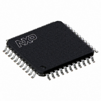
P89V662FBC,557 NXP Semiconductors, P89V662FBC,557 Datasheet - Page 56

P89V662FBC,557
Manufacturer Part Number
P89V662FBC,557
Description
IC 80C51 MCU FLASH 32K 44-TQFP
Manufacturer
NXP Semiconductors
Series
89Vr
Datasheet
1.P89V660FBC557.pdf
(89 pages)
Specifications of P89V662FBC,557
Program Memory Type
FLASH
Program Memory Size
32KB (32K x 8)
Package / Case
44-TQFP
Core Processor
8051
Core Size
8-Bit
Speed
40MHz
Connectivity
I²C, SPI, UART/USART
Peripherals
POR, PWM, WDT
Number Of I /o
36
Ram Size
1K x 8
Voltage - Supply (vcc/vdd)
4.5 V ~ 5.5 V
Oscillator Type
Internal
Operating Temperature
-40°C ~ 85°C
Processor Series
P89V6x
Core
80C51
Data Bus Width
8 bit
Data Ram Size
1 KB
Interface Type
I2C/UART
Maximum Clock Frequency
40 MHz
Number Of Programmable I/os
36
Number Of Timers
3
Operating Supply Voltage
4.5 V to 5.5 V
Maximum Operating Temperature
+ 85 C
Mounting Style
SMD/SMT
3rd Party Development Tools
PK51, CA51, A51, ULINK2
Minimum Operating Temperature
- 40 C
Lead Free Status / RoHS Status
Lead free / RoHS Compliant
For Use With
622-1001 - USB IN-CIRCUIT PROG 80C51ISP
Eeprom Size
-
Data Converters
-
Lead Free Status / Rohs Status
Lead free / RoHS Compliant
Other names
568-2435
935280832557
P89V662FBC
935280832557
P89V662FBC
Available stocks
Company
Part Number
Manufacturer
Quantity
Price
Company:
Part Number:
P89V662FBC,557
Manufacturer:
Maxim
Quantity:
260
Company:
Part Number:
P89V662FBC,557
Manufacturer:
NXP Semiconductors
Quantity:
10 000
NXP Semiconductors
P89V660_662_664_3
Product data sheet
6.10 PCA
6.9 Watchdog timer
The WDT is intended as a recovery method in situations where the CPU may be
subjected to software upset. The WDT consists of a 14-bit counter and the WatchDog
Timer Reset (WDTRST) SFR. The WDT is disabled at reset. To enable the WDT, the user
must write 01EH and 0E1H, in sequence, to the WDTRST SFR. When the WDT is
enabled, it will increment every machine cycle while the oscillator is running and there is
no way to disable the WDT, except through a reset (either hardware reset or a WDT
overflow reset). When the WDT overflows, it will drive an output reset HIGH pulse at the
RST pin.
When the WDT is enabled (and thus running) the user needs to reset it by writing 01EH
and 0E1H, in sequence, to the WDTRST SFR to avoid WDT overflow. The 14-bit counter
reaches overflow when it reaches 16383 (3FFFH) and this will reset the device.
The WDT’s counter cannot be read or written. When the WDT overflows it will generate a
output pulse at the reset pin with a duration of 98 oscillator periods in 6 clock mode or 196
oscillator periods in 12 clock mode.
The PCA includes a special 16-bit Timer that has five 16-bit capture/compare modules
associated with it. Each of the modules can be programmed to operate in one of four
modes: rising and/or falling edge capture, software timer, high-speed output, or pulse
width modulator. Each module has a pin associated with it. Module 0 is connected to
CEX0, module 1 to CEX1, etc. Registers CH and CL contain current value of the free
running up counting 16-bit PCA timer. The PCA timer is a common time base for all five
modules and can be programmed to run at:
frequency, the Timer 0 overflow, or the input on the ECI pin (P1[2]). The timer count
source is determined from the CPS1 and CPS0 bits in the CMOD SFR (see
Table
Fig 25. SPI transfer format with CPHA = 1
46).
SCK (CPOL = 0)
SCK (CPOL = 1)
(for reference)
(from master)
SS (to slave)
SCK cycle #
(from slave)
MOSI
MISO
Rev. 03 — 10 November 2008
MSB
MSB
1
2
6
6
80C51 with 512 B/1 kB/2 kB RAM, dual I
3
5
5
1
4
6
4
4
the oscillator frequency,
5
3
3
P89V660/662/664
6
2
2
7
1
1
LSB
8
© NXP B.V. 2008. All rights reserved.
LSB
1
2
the oscillator
Table 45
002aaa530
2
C-bus, SPI
56 of 89
and


