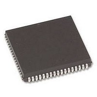
HD6473308RCP10V Renesas Electronics America, HD6473308RCP10V Datasheet - Page 250

HD6473308RCP10V
Manufacturer Part Number
HD6473308RCP10V
Description
MCU 5V 16K,PB-FREE 80-PLCC
Manufacturer
Renesas Electronics America
Series
H8® H8/330r
Datasheet
1.HD6473258P10V.pdf
(349 pages)
Specifications of HD6473308RCP10V
Core Size
8-Bit
Program Memory Size
16KB (16K x 8)
Oscillator Type
Internal
Core Processor
H8/300
Speed
10MHz
Number Of I /o
58
Program Memory Type
OTP
Ram Size
512 x 8
Operating Temperature
-20°C ~ 75°C
Package / Case
80-PLCC
No. Of I/o's
58
Ram Memory Size
512Byte
Cpu Speed
10MHz
No. Of Timers
3
No. Of Pwm Channels
2
Digital Ic Case
RoHS Compliant
Controller Family/series
H8/330
Peripherals
ADC
Rohs Compliant
Yes
Lead Free Status / RoHS Status
Lead free / RoHS Compliant
Voltage - Supply (vcc/vdd)
-
Eeprom Size
-
Data Converters
-
Peripherals
-
Connectivity
-
Lead Free Status / RoHS Status
Lead free / RoHS Compliant
Available stocks
Company
Part Number
Manufacturer
Quantity
Price
Company:
Part Number:
HD6473308RCP10V
Manufacturer:
Renesas Electronics America
Quantity:
10 000
- Current page: 250 of 349
- Download datasheet (2Mb)
Table 12-1. System Control Register
Name
System control register
Bit
Initial value
Read/Write
The only bit in the system control register that concerns the on-chip RAM is the RAME bit. See
section 2.4.2, "System Control Register" for the other bits.
Bit 0 – RAM Enable (RAME): This bit enables or disables the on-chip RAM.
The RAME bit is initialized to “1” on the rising edge of the RES signal, so a reset enables the on-
chip RAM. The RAME bit is not initialized in the software standby mode.
Bit 7
RAME
12.4 Operation
12.4.1 Expanded Modes (Modes 1 and 2)
If the RAME bit is set to “1,” accesses to addresses H’FD80 to H’FF7F are directed to the on-chip
RAM. If the RAME bit is cleared to “0,” accesses to addresses H’FD80 to H’FF7F are directed to
the external data bus.
12.4.2 Single-Chip Mode (Mode 3)
If the RAME bit is set to “1,” accesses to addresses H’FD80 to H’FF7F are directed to the on-chip
RAM.
If the RAME bit is cleared to “0,” the on-chip RAM data cannot be accessed. Attempted write
access has no effect. Attempted read access always results in H’FF data being read.
0
1
Description
On-chip RAM is disabled.
On-chip RAM is enabled.
SSBY
R/W
7
0
STS2
R/W
Abbreviation
SYSCR
6
0
STS1
R/W
5
0
R/W
R/W
STS0
240
R/W
4
0
Initial value
H’09
—
—
3
1
NMIEG DPME
R/W
2
0
Address
H’FFC4
R/W
1
0
(Initial value)
RAME
R/W
0
1
Related parts for HD6473308RCP10V
Image
Part Number
Description
Manufacturer
Datasheet
Request
R

Part Number:
Description:
KIT STARTER FOR M16C/29
Manufacturer:
Renesas Electronics America
Datasheet:

Part Number:
Description:
KIT STARTER FOR R8C/2D
Manufacturer:
Renesas Electronics America
Datasheet:

Part Number:
Description:
R0K33062P STARTER KIT
Manufacturer:
Renesas Electronics America
Datasheet:

Part Number:
Description:
KIT STARTER FOR R8C/23 E8A
Manufacturer:
Renesas Electronics America
Datasheet:

Part Number:
Description:
KIT STARTER FOR R8C/25
Manufacturer:
Renesas Electronics America
Datasheet:

Part Number:
Description:
KIT STARTER H8S2456 SHARPE DSPLY
Manufacturer:
Renesas Electronics America
Datasheet:

Part Number:
Description:
KIT STARTER FOR R8C38C
Manufacturer:
Renesas Electronics America
Datasheet:

Part Number:
Description:
KIT STARTER FOR R8C35C
Manufacturer:
Renesas Electronics America
Datasheet:

Part Number:
Description:
KIT STARTER FOR R8CL3AC+LCD APPS
Manufacturer:
Renesas Electronics America
Datasheet:

Part Number:
Description:
KIT STARTER FOR RX610
Manufacturer:
Renesas Electronics America
Datasheet:

Part Number:
Description:
KIT STARTER FOR R32C/118
Manufacturer:
Renesas Electronics America
Datasheet:

Part Number:
Description:
KIT DEV RSK-R8C/26-29
Manufacturer:
Renesas Electronics America
Datasheet:

Part Number:
Description:
KIT STARTER FOR SH7124
Manufacturer:
Renesas Electronics America
Datasheet:

Part Number:
Description:
KIT STARTER FOR H8SX/1622
Manufacturer:
Renesas Electronics America
Datasheet:

Part Number:
Description:
KIT DEV FOR SH7203
Manufacturer:
Renesas Electronics America
Datasheet:


