HD6417750SF167V Renesas Electronics America, HD6417750SF167V Datasheet - Page 19
HD6417750SF167V
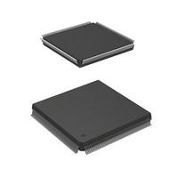
Manufacturer Part Number
HD6417750SF167V
Description
MPU 3V 16K PB-FREE 208-QFP
Manufacturer
Renesas Electronics America
Series
SuperH® SH7750r
Datasheet
1.D6417750RBP240DV.pdf
(1164 pages)
Specifications of HD6417750SF167V
Core Processor
SH-4
Core Size
32-Bit
Speed
167MHz
Connectivity
EBI/EMI, FIFO, SCI, SmartCard
Peripherals
DMA, POR, WDT
Number Of I /o
28
Program Memory Type
ROMless
Ram Size
24K x 8
Voltage - Supply (vcc/vdd)
1.6 V ~ 2 V
Oscillator Type
External
Operating Temperature
-20°C ~ 75°C
Package / Case
208-QFP
Lead Free Status / RoHS Status
Lead free / RoHS Compliant
Eeprom Size
-
Program Memory Size
-
Data Converters
-
Available stocks
Company
Part Number
Manufacturer
Quantity
Price
Company:

Part Number:
HD6417750SF167V
Manufacturer:
INTERSIL
Quantity:
18 720
Company:
Part Number:
HD6417750SF167V
Manufacturer:
Renesas Electronics America
Quantity:
10 000


Item
13.1.2 Block Diagram
Figure 13.1 Block
Diagram of BSC
13.1.3 Pin
Configuration
Table 13.1 BSC Pins
13.1.6 PCMCIA
Support
Table 13.5 PCMCIA
Support Interfaces
13.2.1 Bus Control
Register 1 (BCR1)
13.2.7 Wait Control
Register 3 (WCR3)
Page
359
360
371
372
400
Revision (See Manual for Details)
Figure amended
Table amended
Name
Data bus
Table and notes amended
Pin
59
Note: 1. WP is not supported.
Bit table amended
Initial value:
Description amended
Bits 4n+3⎯Area n (4 or 1) Read-Strobe Negate Timing
(AnRDH) (Setting Only Possible in the SH7750R): When
reading, these bits specify the timing for the negation of read
strobe. These bits should be cleared to 0 when a byte control
SRAM setting is made. Valid only for the SRAM interface.
Bit 4n + 3: AnRDH
0
1
BS
RD/FRAME
RD/WR
WE7–WE0
RAS
CAS7–CAS0, CASS
CKE
ICIORD, ICIOWR
REG
IOIS16
WAIT
Signal
Name
R/W:
Bit:
2. Input an external wait request with correct polarity.
IC Memory Card Interface
Signals
ENDIAN
0/1 *
31
O
R
I/O Function
D63−D52,
D31−D0
1
Wait request
Read-Strobe Negate Timing
Read strobe negated after hold wait cycles specified by WCR3.AnH bits
Read strobe negated according to data sampling timing
MASTER
0/1 *
R
30
1
Rev.7.00 Oct. 10, 2008 Page xvii of lxxxiv
A0MPX
I/O
I/O
0/1 *
29
R
control unit
Memory
1
Signal
Name
WAIT
Description
Data input/output
When port functions are used and DDT mode is
selected, input the DTR format. Otherwise, when
port functions are used, D63−D52 cannot be used
and should be left open.
—
28
0
R
I/O Card Interface
O
I/O Function
27
—
0
R
Wait request
DPUP *
R/W
26
REJ09B0366-0700
0
2
Corresponding
LSI Pin
RDY*
(Initial value)
2
Related parts for HD6417750SF167V
Image
Part Number
Description
Manufacturer
Datasheet
Request
R

Part Number:
Description:
KIT STARTER FOR M16C/29
Manufacturer:
Renesas Electronics America
Datasheet:

Part Number:
Description:
KIT STARTER FOR R8C/2D
Manufacturer:
Renesas Electronics America
Datasheet:

Part Number:
Description:
R0K33062P STARTER KIT
Manufacturer:
Renesas Electronics America
Datasheet:

Part Number:
Description:
KIT STARTER FOR R8C/23 E8A
Manufacturer:
Renesas Electronics America
Datasheet:

Part Number:
Description:
KIT STARTER FOR R8C/25
Manufacturer:
Renesas Electronics America
Datasheet:

Part Number:
Description:
KIT STARTER H8S2456 SHARPE DSPLY
Manufacturer:
Renesas Electronics America
Datasheet:

Part Number:
Description:
KIT STARTER FOR R8C38C
Manufacturer:
Renesas Electronics America
Datasheet:

Part Number:
Description:
KIT STARTER FOR R8C35C
Manufacturer:
Renesas Electronics America
Datasheet:

Part Number:
Description:
KIT STARTER FOR R8CL3AC+LCD APPS
Manufacturer:
Renesas Electronics America
Datasheet:
Part Number:
Description:
KIT STARTER FOR RX610
Manufacturer:
Renesas Electronics America
Datasheet:

Part Number:
Description:
KIT STARTER FOR R32C/118
Manufacturer:
Renesas Electronics America
Datasheet:

Part Number:
Description:
KIT DEV RSK-R8C/26-29
Manufacturer:
Renesas Electronics America
Datasheet:

Part Number:
Description:
KIT STARTER FOR SH7124
Manufacturer:
Renesas Electronics America
Datasheet:

Part Number:
Description:
KIT STARTER FOR H8SX/1622
Manufacturer:
Renesas Electronics America
Datasheet:

Part Number:
Description:
KIT DEV FOR SH7203
Manufacturer:
Renesas Electronics America
Datasheet: