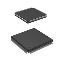
HD6417750SF167V Renesas Electronics America, HD6417750SF167V Datasheet - Page 597

HD6417750SF167V
Manufacturer Part Number
HD6417750SF167V
Description
MPU 3V 16K PB-FREE 208-QFP
Manufacturer
Renesas Electronics America
Series
SuperH® SH7750r
Datasheet
1.D6417750RBP240DV.pdf
(1164 pages)
Specifications of HD6417750SF167V
Core Processor
SH-4
Core Size
32-Bit
Speed
167MHz
Connectivity
EBI/EMI, FIFO, SCI, SmartCard
Peripherals
DMA, POR, WDT
Number Of I /o
28
Program Memory Type
ROMless
Ram Size
24K x 8
Voltage - Supply (vcc/vdd)
1.6 V ~ 2 V
Oscillator Type
External
Operating Temperature
-20°C ~ 75°C
Package / Case
208-QFP
Lead Free Status / RoHS Status
Lead free / RoHS Compliant
Eeprom Size
-
Program Memory Size
-
Data Converters
-
Available stocks
Company
Part Number
Manufacturer
Quantity
Price
Company:
Part Number:
HD6417750SF167V
Manufacturer:
INTERSIL
Quantity:
18 720
Company:
Part Number:
HD6417750SF167V
Manufacturer:
Renesas Electronics America
Quantity:
10 000
- Current page: 597 of 1164
- Download datasheet (7Mb)
13.3.8
If the MD6 pin is set to 0 in a power-on reset by the RESET pin, the MPX interface for normal
memory is selected for area 0. The MPX interface is selected for areas 1 to 6 by means of the
MPX bit in BCR1 and the MEMMODE, A4MPX, and AIMPX bits in BCR3. The MPX interface
offers a multiplexed address/data type bus protocol, and permits easy connection to an external
memory controller chip that uses a single 32-bit multiplexed address/data bus. A bus cycle
consists of an address phase and a data phase. In the address phase, the address information is
output to D25−D0, and the access size to D63−D61 and D31–D29*.
The BS signal which indicates the address phase is asserted for one cycle. The CSn signal is
asserted at the rise of T
negate period does not exist for access with the minimum pitch. The FRAME signal is asserted at
the rise of T
Therefore, in an external device supporting the MPX interface, the address information and access
size output in the address phase must be saved in the external device memory, and data
corresponding to the data phase must be input or output.
For details of access sizes and data alignment, see section 13.3.1, Endian/Access Size and Data
Alignment.
The address pins output at A25–A0 are undefined.
32-byte transfer performed consecutively for a total of 32 bytes according to the set bus width.
The first access is performed on the data for which there was an access request, and the remaining
accesses are performed on the data at the 32-byte boundary. When the access size is larger than the
data bus width, as in this case, burst access is generated, with the address output once, followed by
multiple data cycles. The bus is not released during this period.
Note: * SH7750R only.
D63
0
1
Legend:
X: Don't care
MPX Interface
m1
, and negated when the cycle of the last data transfer starts in the data phase.
D62
0
1
X
m1
, and negated after the last data transfer in the data phase. Therefore, a
D61
0
1
0
1
X
Access Size
Byte
Word
Longword
Quadword
32-byte burst
Rev.7.00 Oct. 10, 2008 Page 511 of 1074
Section 13 Bus State Controller (BSC)
REJ09B0366-0700
Related parts for HD6417750SF167V
Image
Part Number
Description
Manufacturer
Datasheet
Request
R

Part Number:
Description:
KIT STARTER FOR M16C/29
Manufacturer:
Renesas Electronics America
Datasheet:

Part Number:
Description:
KIT STARTER FOR R8C/2D
Manufacturer:
Renesas Electronics America
Datasheet:

Part Number:
Description:
R0K33062P STARTER KIT
Manufacturer:
Renesas Electronics America
Datasheet:

Part Number:
Description:
KIT STARTER FOR R8C/23 E8A
Manufacturer:
Renesas Electronics America
Datasheet:

Part Number:
Description:
KIT STARTER FOR R8C/25
Manufacturer:
Renesas Electronics America
Datasheet:

Part Number:
Description:
KIT STARTER H8S2456 SHARPE DSPLY
Manufacturer:
Renesas Electronics America
Datasheet:

Part Number:
Description:
KIT STARTER FOR R8C38C
Manufacturer:
Renesas Electronics America
Datasheet:

Part Number:
Description:
KIT STARTER FOR R8C35C
Manufacturer:
Renesas Electronics America
Datasheet:

Part Number:
Description:
KIT STARTER FOR R8CL3AC+LCD APPS
Manufacturer:
Renesas Electronics America
Datasheet:

Part Number:
Description:
KIT STARTER FOR RX610
Manufacturer:
Renesas Electronics America
Datasheet:

Part Number:
Description:
KIT STARTER FOR R32C/118
Manufacturer:
Renesas Electronics America
Datasheet:

Part Number:
Description:
KIT DEV RSK-R8C/26-29
Manufacturer:
Renesas Electronics America
Datasheet:

Part Number:
Description:
KIT STARTER FOR SH7124
Manufacturer:
Renesas Electronics America
Datasheet:

Part Number:
Description:
KIT STARTER FOR H8SX/1622
Manufacturer:
Renesas Electronics America
Datasheet:

Part Number:
Description:
KIT DEV FOR SH7203
Manufacturer:
Renesas Electronics America
Datasheet:


