M37542F8FP Renesas Electronics America, M37542F8FP Datasheet - Page 119
M37542F8FP
Manufacturer Part Number
M37542F8FP
Description
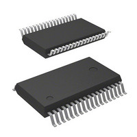
IC 740 MCU FLASH 32K 36SSOP
Manufacturer
Renesas Electronics America
Series
740/38000r
Datasheet
1.M37542F8FPU0.pdf
(124 pages)
Specifications of M37542F8FP
Core Processor
740
Core Size
8-Bit
Speed
8MHz
Connectivity
SIO, UART/USART
Peripherals
POR, WDT
Number Of I /o
29
Program Memory Size
32KB (32K x 8)
Program Memory Type
FLASH
Ram Size
1K x 8
Voltage - Supply (vcc/vdd)
2.2 V ~ 5.5 V
Data Converters
A/D 8x10b
Oscillator Type
Internal
Operating Temperature
-20°C ~ 85°C
Package / Case
36-SSOP
Lead Free Status / RoHS Status
Contains lead / RoHS non-compliant
Eeprom Size
-
Available stocks
Company
Part Number
Manufacturer
Quantity
Price

Part Number:
M37542F8FP
Manufacturer:
MIT
Quantity:
20 000
Company:
Part Number:
M37542F8FP#U0
Manufacturer:
TI
Quantity:
109


7542 Group
Notes on On-chip Oscillation Division Ratio
• When the clock division ratio is switched from f(X
Notes on Oscillation Stop Detection Circuit
1. After the reset by the oscillation stop detection, the value of fol-
lowing bits are retained, not initialized.
• Ceramic or RC oscillation stop detection function active bit
• Oscillation stop detection status bit
2. Oscillation stop detection status bit is initialized (“0”) by the fol-
• External reset
• Write “0” data to the ceramic or RC oscillation stop detection
3. The oscillation stop detection circuit is not included in the emu-
Notes on CPU Rewrite Mode
Take the notes described below when rewriting the flash memory
in CPU rewrite mode.
1. Operation speed
During CPU rewrite mode, set the system clock φ to 4.0 MHz or
less using the clock division ratio selection bits (bits 6 and 7 of
CPU mode register).
2. Instructions inhibited against use
The instructions which refer to the internal data of the flash
memory cannot be used during CPU rewrite mode.
3. Interrupts inhibited against use
The interrupts cannot be used during CPU rewrite mode because
they refer to the internal data of the flash memory.
4. Watchdog timer
If the watchdog timer has been already activated, internal reset
due to an underflow will not occur because the watchdog timer is
surely initialized during program or erase.
5. Reset
Reset is always valid. The MCU is activated using the boot mode
at release of reset in the condition of CNVss = “H”, so that the pro-
gram will begin at the address which is stored in addresses
FFFC
Rev.3.03
REJ03B0006-0303
Bit 1 of MISRG (address 3B
Bit 3 of MISRG
oscillator by the clock division ratio selection bits (bits 7 and 6 of
CPU mode register (address 3B
sion ratio (bits 1 and 0 of on-chip oscillation division ratio
selection register (address 37
middle-speed mode (R
function active bit.
lowing operation.
lator MCU “M37542RSS”.
16
and FFFD
Jul 11, 2008
16
of the boot ROM area.
OSC
/8)).
16
)
Page 117 of 117
16
16
)) is “10
)), the on-chip oscillator divi-
2
” (on-chip oscillator
IN
) to on-chip
Electric Characteristic Differences Between
Mask ROM, Flash Memory MCUs
There are differences in electric characteristics, operation margin,
noise immunity, and noise radiation among mask ROM and flash
memory version MCUs due to the differences in the manufacturing
processes.
When manufacturing an application system with the flash memory
and then switching to use of the mask ROM version, perform suffi-
cient evaluations for the commercial samples of the mask ROM
version.
Note on Power Source Voltage
When the power source voltage value of a microcomputer is less
than the value which is indicated as the recommended operating
conditions, the microcomputer does not operate normally and may
perform unstable operation.
In a system where the power source voltage drops slowly when
the power source voltage drops or the power supply is turned off,
reset a microcomputer when the supply voltage is less than the
recommended operating conditions and design a system not to
cause errors to the system by this unstable operation.
NOTES ON HARDWARE
Handling of Power Source Pin
In order to avoid a latch-up occurrence, connect a capacitor suit-
able for high frequencies as bypass capacitor between power
source pin (Vcc pin) and GND pin (Vss pin). Besides, connect the
capacitor to as close as possible. For bypass capacitor which
should not be located too far from the pins to be connected, a ce-
ramic capacitor of 0.01 µF to 0.1 µF is recommended.
Related parts for M37542F8FP
Image
Part Number
Description
Manufacturer
Datasheet
Request
R

Part Number:
Description:
M37542 EMULATOR KIT (EK) FOR PC4
Manufacturer:
Renesas Electronics America

Part Number:
Description:
KIT STARTER FOR M16C/29
Manufacturer:
Renesas Electronics America
Datasheet:

Part Number:
Description:
KIT STARTER FOR R8C/2D
Manufacturer:
Renesas Electronics America
Datasheet:

Part Number:
Description:
R0K33062P STARTER KIT
Manufacturer:
Renesas Electronics America
Datasheet:

Part Number:
Description:
KIT STARTER FOR R8C/23 E8A
Manufacturer:
Renesas Electronics America
Datasheet:

Part Number:
Description:
KIT STARTER FOR R8C/25
Manufacturer:
Renesas Electronics America
Datasheet:
Part Number:
Description:
KIT STARTER H8S2456 SHARPE DSPLY
Manufacturer:
Renesas Electronics America
Datasheet:

Part Number:
Description:
KIT STARTER FOR R8C38C
Manufacturer:
Renesas Electronics America
Datasheet:

Part Number:
Description:
KIT STARTER FOR R8C35C
Manufacturer:
Renesas Electronics America
Datasheet:

Part Number:
Description:
KIT STARTER FOR R8CL3AC+LCD APPS
Manufacturer:
Renesas Electronics America
Datasheet:
Part Number:
Description:
KIT STARTER FOR RX610
Manufacturer:
Renesas Electronics America
Datasheet:

Part Number:
Description:
KIT STARTER FOR R32C/118
Manufacturer:
Renesas Electronics America
Datasheet:

Part Number:
Description:
KIT DEV RSK-R8C/26-29
Manufacturer:
Renesas Electronics America
Datasheet:

Part Number:
Description:
KIT STARTER FOR SH7124
Manufacturer:
Renesas Electronics America
Datasheet:

Part Number:
Description:
KIT STARTER FOR H8SX/1622
Manufacturer:
Renesas Electronics America
Datasheet: