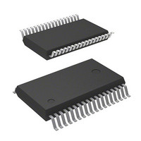
M37542F8FP Renesas Electronics America, M37542F8FP Datasheet - Page 77

M37542F8FP
Manufacturer Part Number
M37542F8FP
Description
IC 740 MCU FLASH 32K 36SSOP
Manufacturer
Renesas Electronics America
Series
740/38000r
Datasheet
1.M37542F8FPU0.pdf
(124 pages)
Specifications of M37542F8FP
Core Processor
740
Core Size
8-Bit
Speed
8MHz
Connectivity
SIO, UART/USART
Peripherals
POR, WDT
Number Of I /o
29
Program Memory Size
32KB (32K x 8)
Program Memory Type
FLASH
Ram Size
1K x 8
Voltage - Supply (vcc/vdd)
2.2 V ~ 5.5 V
Data Converters
A/D 8x10b
Oscillator Type
Internal
Operating Temperature
-20°C ~ 85°C
Package / Case
36-SSOP
Lead Free Status / RoHS Status
Contains lead / RoHS non-compliant
Eeprom Size
-
Available stocks
Company
Part Number
Manufacturer
Quantity
Price
Part Number:
M37542F8FP
Manufacturer:
MIT
Quantity:
20 000
Company:
Part Number:
M37542F8FP#U0
Manufacturer:
TI
Quantity:
109
Fig. 98 Structure of flash memory control register 0
7542 Group
[Flash memory control registers (FMCR0 to FMCR2)]
0FE0
Figure 98 shows the flash memory control register 0.
Bit 0 of the flash memory control register 0 is the RY/BY status
flag used exclusively to read the operating status of the flash
memory. During programming and erase operations, it is “0”
(busy). Otherwise, it is “1” (ready).
Bit 1 of the flash memory control register 0 is the CPU rewrite
mode select bit. When this bit is set to “1”, the MCU enters CPU
rewrite mode. And then, software commands can be accepted. In
CPU rewrite mode, the CPU becomes unable to access the inter-
nal flash memory directly. Therefore, use the control program in
the internal RAM for write to bit 1. To set this bit 1 to “1”, it is nec-
essary to write “0” and then write “1” in succession to bit 1. The bit
can be set to “0” by only writing “0”.
Bit 2 of the flash memory control register 0 is the 8KB user block
E/W mode enable bit. By setting this bit in combination with bit 4
(all user block E/W enable bit) of flash memory control register 2
(address 0FE0
is disabled.
Rev.3.03
REJ03B0006-0303
16
to 0FE2
Jul 11, 2008
16
16
), Erase/Write to user block in CPU rewrite mode
b7
Page 75 of 117
Notes 1: For this bit to be set to “1”, the user needs to write a “0” and then a
2: This bit can be written only when CPU rewrite mode select bit is “1”.
3: Effective only when the CPU rewrite mode select bit = “1”. Fix this
4: Write to this bit in program on RAM
“1” to it in succession. For this bit to be set to “0”, write “0” only to
this bit.
bit to “0” when the CPU rewrite mode select bit is “0”.
b0
Flash memory control register 0
(FMCR0: address : 0FE0
CPU rewrite mode select bit (Note 1)
0 :
1 :
8KB user block E/W mode enable bit
0 : E/W disabled
1 : E/W enabled
Flash memory reset bit
0 : Normal operation
1 : reset
Not used (do not write “1” to this bit.)
User ROM area select bit
0 : Boot ROM area is accessed
1 : User ROM area is accessed
Erase status flag
0: Pass
1: Error
Program status flag
0: Pass
1: Error
RY/BY
0 : Busy (being written or erased)
1 : Ready
CPU rewrite mode
CPU rewrite mode valid
status flag
Bit 3 of the flash memory control register 0 is the flash memory re-
set bit used to reset the control circuit of internal flash memory.
This bit is used when exiting CPU rewrite mode and when flash
memory access has failed. When the CPU rewrite mode select bit
is “1”, setting “1” for this bit resets the control circuit. To release
the reset, it is necessary to set this bit to “0”.
Bit 5 of the flash memory control register 0 is the User ROM area
select bit and is valid only in the boot mode. Setting this bit to “1”
in the boot mode switches an accessible area from the boot ROM
area to the user ROM area. To use the CPU rewrite mode in the
boot mode, set this bit to “1”. Note that when the microcomputer is
booted up in the user ROM area, only the user ROM area is ac-
cessible and bit 5 is invalid; on the other hand, when the
microcomputer is in the boot mode, bit 5 is valid independent of
the CPU rewrite mode. To rewrite bit 5, execute the user-original
reprogramming control software transferred to the internal RAM in
advance.
Bit 6 of the flash memory control register 0 is the program status
flag. This bit is set to “1” when writing to flash memory is failed.
When program error occurs, the block cannot be used.
Bit 7 of the flash memory control register 0 is the erase status flag.
This bit is set to “1” when erasing flash memory is failed. When
erase error occurs, the block cannot be used.
(Note 3)
invalid
16
(Note 4)
: initial value: 01
(Note 1, 2)
16
)


