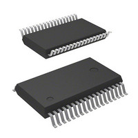
M37542F8FP Renesas Electronics America, M37542F8FP Datasheet - Page 49

M37542F8FP
Manufacturer Part Number
M37542F8FP
Description
IC 740 MCU FLASH 32K 36SSOP
Manufacturer
Renesas Electronics America
Series
740/38000r
Datasheet
1.M37542F8FPU0.pdf
(124 pages)
Specifications of M37542F8FP
Core Processor
740
Core Size
8-Bit
Speed
8MHz
Connectivity
SIO, UART/USART
Peripherals
POR, WDT
Number Of I /o
29
Program Memory Size
32KB (32K x 8)
Program Memory Type
FLASH
Ram Size
1K x 8
Voltage - Supply (vcc/vdd)
2.2 V ~ 5.5 V
Data Converters
A/D 8x10b
Oscillator Type
Internal
Operating Temperature
-20°C ~ 85°C
Package / Case
36-SSOP
Lead Free Status / RoHS Status
Contains lead / RoHS non-compliant
Eeprom Size
-
Available stocks
Company
Part Number
Manufacturer
Quantity
Price
Part Number:
M37542F8FP
Manufacturer:
MIT
Quantity:
20 000
Company:
Part Number:
M37542F8FP#U0
Manufacturer:
TI
Quantity:
109
Fig. 56 Operation of clock synchronous serial I/O1 function
7542 Group
Serial Interface
The 7542 Group has Serial I/O1 and Serial I/O2. Except that Serial
I/O1 has the bus collision detection function and the T
structure for Serial I/O2 is CMOS only, they have the same function.
Serial I/O1 can be used as either clock synchronous or asynchro-
nous (UART) serial I/O. A dedicated timer is also provided for
baud rate generation.
Fig. 55 Block diagram of clock synchronous serial I/O1
Rev.3.03
REJ03B0006-0303
Serial I/O1
Write pulse to receive/transmit
buffer register 1 (address 0018
Receive enable signal S
Transfer shift clock
(1/2 to 1/2048 of the internal
clock, or an external clock)
Notes 1: As the transmit interrupt (TI), which can be selected, either when the transmit buffer has emptied (TBE=1) or after
P 1
P 1
X
P 1
P 1
IN
0
2
3
1
Jul 11, 2008
/ R
/ S
/ S
/ T
2: If data is written to the transmit buffer register when TSC=0, the transmit clock is generated continuously and serial
3: The receive interrupt (RI) is set when the receive buffer full flag (RBF) becomes “1” .
Serial output TxD
Serial input RxD
C L K 1
R D Y 1
X
X
the transmit shift operation has ended (TSC=1), by setting the transmit interrupt source selection bit (TIC) of the
serial I/O1 control register.
data is output continuously from the TxD
D
D
1
1
/ C A P
0
RDY1
BRG count source selection bit
F / F
1
1
16
Page 47 of 117
)
TBE = 0
1 / 4
Falling-edge detector
TBE = 1
TSC = 0
D
D
0
0
Receive buffer register 1
R e c e i v e s h i f t r e g i s t e r 1
1
X
pin.
D
2
Transmit shift register 1
T r a n s m i t b u f f e r r e g i s t e r 1
D
D
Data bus
output
Data bus
1
1
A d d r e s s 0 0 1 8
S h i f t c l o c k
Serial I/O1 synchronous
clock selection bit
Frequency division ratio 1/(n+1)
Baud rate generator 1
A d d r e s s 0 0 1 8
D
D
Shift clock
Address 001C
2
2
(1) Clock Synchronous Serial I/O1 Mode
Clock synchronous serial I/O1 mode can be selected by setting
the serial I/O1 mode selection bit of the serial I/O1 control register
(bit 6) to “1”.
For clock synchronous serial I/O1, the transmitter and the receiver
must use the same clock. If an internal clock is used, transfer is
started by a write signal to the TB/RB.
1 6
D
D
3
3
C l o c k c o n t r o l c i r c u i t
1 6
Clock control circuit
16
Serial I/O1 control register
Transmit interrupt source selection bit
R e c e i v e b u f f e r f u l l f l a g ( R B F )
S e r i a l I / O 1 s t a t u s r e g i s t e r
D
D
1 / 4
4
4
Receive interrupt request (RI)
D
D
5
5
T r a n s m i t s h i f t c o m p l e t i o n f l a g ( T S C )
T r a n s m i t b u f f e r e m p t y f l a g ( T B E )
T r a n s m i t i n t e r r u p t r e q u e s t ( T I )
D
D
6
6
A d d r e s s 0 0 1 A
Overrun error (OE)
detection
Address 0019
RBF = 1
TSC = 1
D
D
7
7
1 6
16


