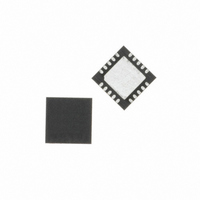
C8051F537-IM Silicon Laboratories Inc, C8051F537-IM Datasheet - Page 124

C8051F537-IM
Manufacturer Part Number
C8051F537-IM
Description
IC 8051 MCU 2K FLASH 20QFN
Manufacturer
Silicon Laboratories Inc
Series
C8051F53xr
Specifications of C8051F537-IM
Core Processor
8051
Core Size
8-Bit
Speed
25MHz
Connectivity
SPI, UART/USART
Peripherals
Brown-out Detect/Reset, POR, PWM, Temp Sensor, WDT
Number Of I /o
16
Program Memory Size
2KB (2K x 8)
Program Memory Type
FLASH
Ram Size
256 x 8
Voltage - Supply (vcc/vdd)
2 V ~ 5.25 V
Data Converters
A/D 16x12b
Oscillator Type
Internal
Operating Temperature
-40°C ~ 125°C
Package / Case
20-QFN
Data Bus Width
8 bit
Data Ram Size
256 B
Interface Type
SPI, UART
Maximum Clock Frequency
25 MHz
Number Of Programmable I/os
16
Number Of Timers
3
Operating Supply Voltage
2.7 V to 5.25 V
Maximum Operating Temperature
+ 125 C
Mounting Style
SMD/SMT
Minimum Operating Temperature
- 40 C
On-chip Adc
12 bit, 16 Channel
Lead Free Status / RoHS Status
Lead free / RoHS Compliant
Eeprom Size
-
Lead Free Status / Rohs Status
Details
Other names
336-1400
Available stocks
Company
Part Number
Manufacturer
Quantity
Price
Company:
Part Number:
C8051F537-IM
Manufacturer:
Silicon Labs
Quantity:
135
- Current page: 124 of 218
- Download datasheet (2Mb)
C8051F52x/F52xA/F53x/F53xA
Registers XBR0 and XBR1 are used to assign the digital I/O resources to the physical I/O Port pins. Note
that when the SMBus is selected, the Crossbar assigns both pins associated with the SMBus (SDA and
SCL); when the UART is selected, the Crossbar assigns both pins associated with the UART (TX and RX).
UART0 pin assignments are fixed for bootloading purposes: UART TX0 is always assigned to P0.3 or
P0.4*; UART RX0 is always assigned to P0.4 or P0.5*. Standard Port I/Os appear contiguously starting at
P0.0 after prioritized functions and skipped pins are assigned.
Note: Refer to Section “20. Device Specific Behavior” on page 209.
124
Figure 13.6. Crossbar Priority Decoder with Some Pins Skipped (DFN 10)
Note: 4-Wire SPI Only.
SF Signals DFN 10
PIN I/O
TX0
RX0
TX0
RX0
SCK
MISO
MOSI
NSS*
LIN-TX
LIN-RX
CP0
CP0A
/SYSCLK
CEX0
CEX1
CEX2
ECI
T0
T1
SF Signals
Port pin potentially assignable to peripheral
Special Function Signals are not assigned by the crossbar.
When these signals are enabled, the Crossbar must be manually configured
to skip their corresponding port pins.
0
0
P0SKIP[0:5] = 0x06
1
1
2
1
P0
3
0
4
0
Rev. 1.3
5
0
C8051F52xA devices
C8051F52x devices
Related parts for C8051F537-IM
Image
Part Number
Description
Manufacturer
Datasheet
Request
R
Part Number:
Description:
SMD/C°/SINGLE-ENDED OUTPUT SILICON OSCILLATOR
Manufacturer:
Silicon Laboratories Inc
Part Number:
Description:
Manufacturer:
Silicon Laboratories Inc
Datasheet:
Part Number:
Description:
N/A N/A/SI4010 AES KEYFOB DEMO WITH LCD RX
Manufacturer:
Silicon Laboratories Inc
Datasheet:
Part Number:
Description:
N/A N/A/SI4010 SIMPLIFIED KEY FOB DEMO WITH LED RX
Manufacturer:
Silicon Laboratories Inc
Datasheet:
Part Number:
Description:
N/A/-40 TO 85 OC/EZLINK MODULE; F930/4432 HIGH BAND (REV E/B1)
Manufacturer:
Silicon Laboratories Inc
Part Number:
Description:
EZLink Module; F930/4432 Low Band (rev e/B1)
Manufacturer:
Silicon Laboratories Inc
Part Number:
Description:
I°/4460 10 DBM RADIO TEST CARD 434 MHZ
Manufacturer:
Silicon Laboratories Inc
Part Number:
Description:
I°/4461 14 DBM RADIO TEST CARD 868 MHZ
Manufacturer:
Silicon Laboratories Inc
Part Number:
Description:
I°/4463 20 DBM RFSWITCH RADIO TEST CARD 460 MHZ
Manufacturer:
Silicon Laboratories Inc
Part Number:
Description:
I°/4463 20 DBM RADIO TEST CARD 868 MHZ
Manufacturer:
Silicon Laboratories Inc
Part Number:
Description:
I°/4463 27 DBM RADIO TEST CARD 868 MHZ
Manufacturer:
Silicon Laboratories Inc
Part Number:
Description:
I°/4463 SKYWORKS 30 DBM RADIO TEST CARD 915 MHZ
Manufacturer:
Silicon Laboratories Inc
Part Number:
Description:
N/A N/A/-40 TO 85 OC/4463 RFMD 30 DBM RADIO TEST CARD 915 MHZ
Manufacturer:
Silicon Laboratories Inc
Part Number:
Description:
I°/4463 20 DBM RADIO TEST CARD 169 MHZ
Manufacturer:
Silicon Laboratories Inc


