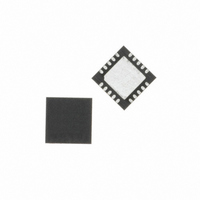
C8051F537-IM Silicon Laboratories Inc, C8051F537-IM Datasheet - Page 74

C8051F537-IM
Manufacturer Part Number
C8051F537-IM
Description
IC 8051 MCU 2K FLASH 20QFN
Manufacturer
Silicon Laboratories Inc
Series
C8051F53xr
Specifications of C8051F537-IM
Core Processor
8051
Core Size
8-Bit
Speed
25MHz
Connectivity
SPI, UART/USART
Peripherals
Brown-out Detect/Reset, POR, PWM, Temp Sensor, WDT
Number Of I /o
16
Program Memory Size
2KB (2K x 8)
Program Memory Type
FLASH
Ram Size
256 x 8
Voltage - Supply (vcc/vdd)
2 V ~ 5.25 V
Data Converters
A/D 16x12b
Oscillator Type
Internal
Operating Temperature
-40°C ~ 125°C
Package / Case
20-QFN
Data Bus Width
8 bit
Data Ram Size
256 B
Interface Type
SPI, UART
Maximum Clock Frequency
25 MHz
Number Of Programmable I/os
16
Number Of Timers
3
Operating Supply Voltage
2.7 V to 5.25 V
Maximum Operating Temperature
+ 125 C
Mounting Style
SMD/SMT
Minimum Operating Temperature
- 40 C
On-chip Adc
12 bit, 16 Channel
Lead Free Status / RoHS Status
Lead free / RoHS Compliant
Eeprom Size
-
Lead Free Status / Rohs Status
Details
Other names
336-1400
Available stocks
Company
Part Number
Manufacturer
Quantity
Price
Company:
Part Number:
C8051F537-IM
Manufacturer:
Silicon Labs
Quantity:
135
- Current page: 74 of 218
- Download datasheet (2Mb)
C8051F52x/F52xA/F53x/F53xA
6. Voltage Regulator (REG0)
C8051F52x/F52xA/F53x/F53xAdevices include an on-chip low dropout voltage regulator (REG0). The
input to REG0 at the V
or 2.6 V. When enabled, the output of REG0 appears on the V
can be used to power external devices. On reset, REG0 is enabled and can be disabled by software.
The input (V
tor (4.7 µF + 0.1 µF) to ground. This capacitor will eliminate power spikes and provide any immediate
power required by the microcontroller. The settling time associated with the voltage regulator is shown in
Table 2.5 on page 30.
The voltage regulator can also generate an interrupt (if enabled by EREG0, EIE1.6) that is triggered when-
ever the V
interrupt has no pending flag. The recommended procedure to use the interrupt is as follows:
1. Wait enough time to ensure the V
2. Enable the dropout interrupt (EREG0, EIE1.6) and select the proper priority (PREG0, EIP1.6).
3. If triggered, disable the interrupt in the Interrupt Service Routine (clear EREG0, EIE1.6) and execute all
4. The main application, now running in safe mode, should regularly check the DROPOUT bit
74
necessary procedures to put the system in “safe mode,” leaving the interrupt disabled.
(REG0CN.0). Once it is cleared by the regulator hardware, the application can re-enable the interrupt
(EREG0, EIE1.6) and return to normal mode operation.
REGIN
REGIN
Figure 6.1. External Capacitors for Voltage Regulator Input/Output
input voltage drops below the dropout threshold (see Table 2.5 on page 30). This dropout
) and output (V
REGIN
REG0
V
DD
pin can be as high as 5.25 V. The output can be selected by software to 2.1 V
4.7 µF
4.7 µF
DD
) of the voltage regulator should both be bypassed with a large capaci-
REGIN
input voltage is stable.
Rev. 1.3
.1 µF
.1 µF
DD
pin, powers the microcontroller core, and
VREGIN
V
DD
Related parts for C8051F537-IM
Image
Part Number
Description
Manufacturer
Datasheet
Request
R
Part Number:
Description:
SMD/C°/SINGLE-ENDED OUTPUT SILICON OSCILLATOR
Manufacturer:
Silicon Laboratories Inc
Part Number:
Description:
Manufacturer:
Silicon Laboratories Inc
Datasheet:
Part Number:
Description:
N/A N/A/SI4010 AES KEYFOB DEMO WITH LCD RX
Manufacturer:
Silicon Laboratories Inc
Datasheet:
Part Number:
Description:
N/A N/A/SI4010 SIMPLIFIED KEY FOB DEMO WITH LED RX
Manufacturer:
Silicon Laboratories Inc
Datasheet:
Part Number:
Description:
N/A/-40 TO 85 OC/EZLINK MODULE; F930/4432 HIGH BAND (REV E/B1)
Manufacturer:
Silicon Laboratories Inc
Part Number:
Description:
EZLink Module; F930/4432 Low Band (rev e/B1)
Manufacturer:
Silicon Laboratories Inc
Part Number:
Description:
I°/4460 10 DBM RADIO TEST CARD 434 MHZ
Manufacturer:
Silicon Laboratories Inc
Part Number:
Description:
I°/4461 14 DBM RADIO TEST CARD 868 MHZ
Manufacturer:
Silicon Laboratories Inc
Part Number:
Description:
I°/4463 20 DBM RFSWITCH RADIO TEST CARD 460 MHZ
Manufacturer:
Silicon Laboratories Inc
Part Number:
Description:
I°/4463 20 DBM RADIO TEST CARD 868 MHZ
Manufacturer:
Silicon Laboratories Inc
Part Number:
Description:
I°/4463 27 DBM RADIO TEST CARD 868 MHZ
Manufacturer:
Silicon Laboratories Inc
Part Number:
Description:
I°/4463 SKYWORKS 30 DBM RADIO TEST CARD 915 MHZ
Manufacturer:
Silicon Laboratories Inc
Part Number:
Description:
N/A N/A/-40 TO 85 OC/4463 RFMD 30 DBM RADIO TEST CARD 915 MHZ
Manufacturer:
Silicon Laboratories Inc
Part Number:
Description:
I°/4463 20 DBM RADIO TEST CARD 169 MHZ
Manufacturer:
Silicon Laboratories Inc


