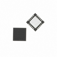
C8051F537-IM Silicon Laboratories Inc, C8051F537-IM Datasheet - Page 61

C8051F537-IM
Manufacturer Part Number
C8051F537-IM
Description
IC 8051 MCU 2K FLASH 20QFN
Manufacturer
Silicon Laboratories Inc
Series
C8051F53xr
Specifications of C8051F537-IM
Core Processor
8051
Core Size
8-Bit
Speed
25MHz
Connectivity
SPI, UART/USART
Peripherals
Brown-out Detect/Reset, POR, PWM, Temp Sensor, WDT
Number Of I /o
16
Program Memory Size
2KB (2K x 8)
Program Memory Type
FLASH
Ram Size
256 x 8
Voltage - Supply (vcc/vdd)
2 V ~ 5.25 V
Data Converters
A/D 16x12b
Oscillator Type
Internal
Operating Temperature
-40°C ~ 125°C
Package / Case
20-QFN
Data Bus Width
8 bit
Data Ram Size
256 B
Interface Type
SPI, UART
Maximum Clock Frequency
25 MHz
Number Of Programmable I/os
16
Number Of Timers
3
Operating Supply Voltage
2.7 V to 5.25 V
Maximum Operating Temperature
+ 125 C
Mounting Style
SMD/SMT
Minimum Operating Temperature
- 40 C
On-chip Adc
12 bit, 16 Channel
Lead Free Status / RoHS Status
Lead free / RoHS Compliant
Eeprom Size
-
Lead Free Status / Rohs Status
Details
Other names
336-1400
Available stocks
Company
Part Number
Manufacturer
Quantity
Price
Company:
Part Number:
C8051F537-IM
Manufacturer:
Silicon Labs
Quantity:
135
- Current page: 61 of 218
- Download datasheet (2Mb)
4.4.1. Calculating the Gain Value
The ADC0 selectable gain feature is controlled by 13 bits in three registers. ADC0GNH contains the 8
upper bits of the gain value and ADC0GNL contains the 4 lower bits of the gain value. The final GAINADD
bit (ADC0GNA.0) controls an optional extra 1/64 (0.016) of gain that can be added in addition to the
ADC0GNH and ADC0GNL gain. The ADC0GNA.0 bit is set to 1 after a power-on reset.
The equivalent gain for the ADC0GNH, ADC0GNL and ADC0GNA registers is:
Where:
GAIN is the 12-bit word of ADC0GNH[7:0] and ADC0GNL[7:4]
GAINADD is the value of the GAINADD bit (ADC0GNA.0)
gain is the equivalent gain value from 0 to 1.016
For example, if ADC0GNH = 0xFC, ADC0GNL = 0x00, and GAINADD = '1', GAIN = 0xFC0 = 4032, and
the resulting equation is:
The table below equates values in the ADC0GNH, ADC0GNL, and ADC0GNA registers to the equivalent
gain using this equation.
For any desired gain value, the GAIN registers can be calculated by:
Where:
GAIN is the 12-bit word of ADC0GNH[7:0] and ADC0GNL[7:4]
GAINADD is the value of the GAINADD bit (ADC0GNA.0)
gain is the equivalent gain value from 0 to 1.016
When calculating the value of GAIN to load into the ADC0GNH and ADC0GNL registers, the GAINADD bit
can be turned on or off to reach a value closer to the desired gain value.
ADC0GNH Value
Equation 4.3. Calculating the ADC0GNH and ADC0GNL Values from the Desired Gain
0xFC (default)
0xBC
0x7C
0x3C
0xFF
0xFF
Equation 4.2. Equivalent Gain from the ADC0GNH and ADC0GNL Registers
gain
ADC0GNL Value
0x00 (default)
GAIN
=
gain
0xF0
0xF0
0x00
0x00
0x00
4032
----------- -
4096
=
=
gain GAINADD
GAIN
-------------- -
+
4096
C8051F52x/F52xA/F53x/F53xA
1
–
GAINADD Value
1 (default)
----- -
64
1
+
Rev. 1.3
GAINADD
1
1
1
0
1
=
0.984
----- -
64
+
1
0.016
----- -
64
GAIN Value
1
4032 + 64
1984 + 64
3008 + 64
4095 + 64
960 + 64
4095 + 0
4096
=
1.0
Equivalent Gain
1.0 (default)
1.016
0.75
0.25
~1.0
0.5
61
Related parts for C8051F537-IM
Image
Part Number
Description
Manufacturer
Datasheet
Request
R
Part Number:
Description:
SMD/C°/SINGLE-ENDED OUTPUT SILICON OSCILLATOR
Manufacturer:
Silicon Laboratories Inc
Part Number:
Description:
Manufacturer:
Silicon Laboratories Inc
Datasheet:
Part Number:
Description:
N/A N/A/SI4010 AES KEYFOB DEMO WITH LCD RX
Manufacturer:
Silicon Laboratories Inc
Datasheet:
Part Number:
Description:
N/A N/A/SI4010 SIMPLIFIED KEY FOB DEMO WITH LED RX
Manufacturer:
Silicon Laboratories Inc
Datasheet:
Part Number:
Description:
N/A/-40 TO 85 OC/EZLINK MODULE; F930/4432 HIGH BAND (REV E/B1)
Manufacturer:
Silicon Laboratories Inc
Part Number:
Description:
EZLink Module; F930/4432 Low Band (rev e/B1)
Manufacturer:
Silicon Laboratories Inc
Part Number:
Description:
I°/4460 10 DBM RADIO TEST CARD 434 MHZ
Manufacturer:
Silicon Laboratories Inc
Part Number:
Description:
I°/4461 14 DBM RADIO TEST CARD 868 MHZ
Manufacturer:
Silicon Laboratories Inc
Part Number:
Description:
I°/4463 20 DBM RFSWITCH RADIO TEST CARD 460 MHZ
Manufacturer:
Silicon Laboratories Inc
Part Number:
Description:
I°/4463 20 DBM RADIO TEST CARD 868 MHZ
Manufacturer:
Silicon Laboratories Inc
Part Number:
Description:
I°/4463 27 DBM RADIO TEST CARD 868 MHZ
Manufacturer:
Silicon Laboratories Inc
Part Number:
Description:
I°/4463 SKYWORKS 30 DBM RADIO TEST CARD 915 MHZ
Manufacturer:
Silicon Laboratories Inc
Part Number:
Description:
N/A N/A/-40 TO 85 OC/4463 RFMD 30 DBM RADIO TEST CARD 915 MHZ
Manufacturer:
Silicon Laboratories Inc
Part Number:
Description:
I°/4463 20 DBM RADIO TEST CARD 169 MHZ
Manufacturer:
Silicon Laboratories Inc


