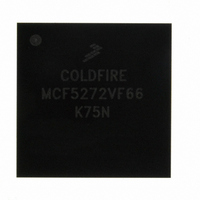
MCF5272VF66 Freescale Semiconductor, MCF5272VF66 Datasheet - Page 120

MCF5272VF66
Manufacturer Part Number
MCF5272VF66
Description
IC MPU 32BIT 66MHZ 196-MAPBGA
Manufacturer
Freescale Semiconductor
Series
MCF527xr
Specifications of MCF5272VF66
Core Processor
Coldfire V2
Core Size
32-Bit
Speed
66MHz
Connectivity
EBI/EMI, Ethernet, I²C, SPI, UART/USART, USB
Peripherals
DMA, WDT
Number Of I /o
32
Program Memory Size
16KB (4K x 32)
Program Memory Type
ROM
Ram Size
1K x 32
Voltage - Supply (vcc/vdd)
3 V ~ 3.6 V
Oscillator Type
External
Operating Temperature
0°C ~ 70°C
Package / Case
196-MAPBGA
Lead Free Status / RoHS Status
Contains lead / RoHS non-compliant
Eeprom Size
-
Data Converters
-
Available stocks
Company
Part Number
Manufacturer
Quantity
Price
Company:
Part Number:
MCF5272VF66
Manufacturer:
HYNIX
Quantity:
19
Company:
Part Number:
MCF5272VF66
Manufacturer:
FREESCAL
Quantity:
885
Company:
Part Number:
MCF5272VF66
Manufacturer:
Freescale Semiconductor
Quantity:
10 000
Part Number:
MCF5272VF66
Manufacturer:
FREESCALE
Quantity:
20 000
Company:
Part Number:
MCF5272VF66J
Manufacturer:
Freescale
Quantity:
256
Company:
Part Number:
MCF5272VF66J
Manufacturer:
Freescale Semiconductor
Quantity:
10 000
Company:
Part Number:
MCF5272VF66R2
Manufacturer:
Freescale Semiconductor
Quantity:
10 000
Company:
Part Number:
MCF5272VF66R2J
Manufacturer:
Freescale Semiconductor
Quantity:
10 000
- Current page: 120 of 544
- Download datasheet (7Mb)
Debug Support
5.2
Table 5-1
rising edge of the processor core’s clock signal. The standard 26-pin debug connector is shown in
Section 5.8, “Freescale-Recommended BDM
Figure 5-2
5-2
Development Serial
Clock (DSCLK)
Development Serial
Input (DSI)
Development Serial
Output (DSO)
Breakpoint (BKPT)
Processor Status
Clock (PSTCLK)
Debug Data
(DDATA[3:0])
Processor Status
(PST[3:0])
Signal
Signal Description
describes debug module signals. All ColdFire debug signals are unidirectional and related to a
shows PSTCLK timing with respect to PST and DDATA.
PST
or
PSTCLK
DDATA
Internally synchronized input. (The logic level on DSCLK is validated if it has the same value on two
consecutive rising CLKIN edges.) Clocks the serial communication port to the debug module during
packet transfers. Maximum frequency is 1/5 the processor status clock (PSTCLK) speed. At the
synchronized rising edge of DSCLK, the data input on DSI is sampled and DSO changes state.
Internally synchronized input that provides data input for the serial communication port to the debug
module.
Provides serial output communication for debug module responses. DSO is registered internally.
Input used to request a manual breakpoint. Assertion of BKPT puts the processor into a halted state
after the current instruction completes. Halt status is reflected on processor status signals (PST[3:0]) as
the value 0xF.
Delayed version of the processor clock. Its rising edge appears in the center of valid PST and DDATA
output. See
DDATA values.
These output signals display the register breakpoint status as a default, or optionally, captured address
and operand values. The capturing of data values is controlled by the setting of the CSR. Additionally,
execution of the WDDATA instruction by the processor captures operands which are displayed on
DDATA. These signals are updated each processor cycle.
These output signals report the processor status.
outputs indicate the current status of the processor pipeline and, as a result, are not related to the
current bus transfer. The PST value is updated each processor cycle.
MCF5272 ColdFire
Figure
5-2. PSTCLK indicates when the development system should sample PST and
Table 5-1. Debug Module Signals
®
Figure 5-2. PSTCLK Timing
Integrated Microprocessor User’s Manual, Rev. 3
Pinout.”
Description
Table 5-2
shows the encoding of these signals. These
Freescale Semiconductor
Related parts for MCF5272VF66
Image
Part Number
Description
Manufacturer
Datasheet
Request
R
Part Number:
Description:
Mcf5272 Coldfire Integrated Microprocessor User
Manufacturer:
Freescale Semiconductor, Inc
Datasheet:

Part Number:
Description:
MCF5272 Interrupt Service Routine for the Physical Layer Interface Controller
Manufacturer:
Freescale Semiconductor / Motorola
Datasheet:
Part Number:
Description:
Manufacturer:
Freescale Semiconductor, Inc
Datasheet:
Part Number:
Description:
Manufacturer:
Freescale Semiconductor, Inc
Datasheet:
Part Number:
Description:
Manufacturer:
Freescale Semiconductor, Inc
Datasheet:
Part Number:
Description:
Manufacturer:
Freescale Semiconductor, Inc
Datasheet:
Part Number:
Description:
Manufacturer:
Freescale Semiconductor, Inc
Datasheet:
Part Number:
Description:
Manufacturer:
Freescale Semiconductor, Inc
Datasheet:
Part Number:
Description:
Manufacturer:
Freescale Semiconductor, Inc
Datasheet:
Part Number:
Description:
Manufacturer:
Freescale Semiconductor, Inc
Datasheet:
Part Number:
Description:
Manufacturer:
Freescale Semiconductor, Inc
Datasheet:
Part Number:
Description:
Manufacturer:
Freescale Semiconductor, Inc
Datasheet:
Part Number:
Description:
Manufacturer:
Freescale Semiconductor, Inc
Datasheet:
Part Number:
Description:
Manufacturer:
Freescale Semiconductor, Inc
Datasheet:
Part Number:
Description:
Manufacturer:
Freescale Semiconductor, Inc
Datasheet:


