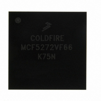
MCF5272VF66 Freescale Semiconductor, MCF5272VF66 Datasheet - Page 203

MCF5272VF66
Manufacturer Part Number
MCF5272VF66
Description
IC MPU 32BIT 66MHZ 196-MAPBGA
Manufacturer
Freescale Semiconductor
Series
MCF527xr
Specifications of MCF5272VF66
Core Processor
Coldfire V2
Core Size
32-Bit
Speed
66MHz
Connectivity
EBI/EMI, Ethernet, I²C, SPI, UART/USART, USB
Peripherals
DMA, WDT
Number Of I /o
32
Program Memory Size
16KB (4K x 32)
Program Memory Type
ROM
Ram Size
1K x 32
Voltage - Supply (vcc/vdd)
3 V ~ 3.6 V
Oscillator Type
External
Operating Temperature
0°C ~ 70°C
Package / Case
196-MAPBGA
Lead Free Status / RoHS Status
Contains lead / RoHS non-compliant
Eeprom Size
-
Data Converters
-
Available stocks
Company
Part Number
Manufacturer
Quantity
Price
Company:
Part Number:
MCF5272VF66
Manufacturer:
HYNIX
Quantity:
19
Company:
Part Number:
MCF5272VF66
Manufacturer:
FREESCAL
Quantity:
885
Company:
Part Number:
MCF5272VF66
Manufacturer:
Freescale Semiconductor
Quantity:
10 000
Part Number:
MCF5272VF66
Manufacturer:
FREESCALE
Quantity:
20 000
Company:
Part Number:
MCF5272VF66J
Manufacturer:
Freescale
Quantity:
256
Company:
Part Number:
MCF5272VF66J
Manufacturer:
Freescale Semiconductor
Quantity:
10 000
Company:
Part Number:
MCF5272VF66R2
Manufacturer:
Freescale Semiconductor
Quantity:
10 000
Company:
Part Number:
MCF5272VF66R2J
Manufacturer:
Freescale Semiconductor
Quantity:
10 000
- Current page: 203 of 544
- Download datasheet (7Mb)
As
be refined by setting SDCR[INV], which inverts the SDRAM clock. SDCR[REG] must always be cleared
when SDCR[INV] is set.
The incoming data setup time should be inspected during reads. The active clock edge event of SDCLK
now precedes the MCF5272 internal active clock edge event when (REG = 0). This behavior is frequency
dependent. The two following scenarios are possible:
If the delay between shifted SDCLK and following internal system clock edge is shorter than the read
access time of the SDRAM, data is sampled with the true CAS latency.
Freescale Semiconductor
.
Figure 9-6
•
•
Internal
High-speed timing refinement with true CAS latency. See
Low-speed timing refinement with reduced effective CAS latency.
Internal CLK
SDCLK
Data bus
SDCLK
Data
CLK
shows timing relationships between SDCLK and the remaining data and control signals can
If the delay difference between the fastest data signal and the slowest control
signal exceeds half of the clock cycle time, the clock shift can cause
hold-time violations on control signals.
Figure 9-7. Timing Refinement with True CAS Latency and Inverted SDCLK
MCF5272 ColdFire
Figure 9-6. Timing Refinement with Inverted SDCLK
®
Integrated Microprocessor User’s Manual, Rev. 3
Data setup delay
NOTE
Shifted delay of SDCLK
CASL = 2
T
SDCLK_to_CLK
Shifted delay of SDCLK
- T
Figure
acc
< 0 => true CAS latency
Delay SDCLK to CLK
9-7.
SDRAM read access time
SDRAM Controller
9-13
Related parts for MCF5272VF66
Image
Part Number
Description
Manufacturer
Datasheet
Request
R
Part Number:
Description:
Mcf5272 Coldfire Integrated Microprocessor User
Manufacturer:
Freescale Semiconductor, Inc
Datasheet:

Part Number:
Description:
MCF5272 Interrupt Service Routine for the Physical Layer Interface Controller
Manufacturer:
Freescale Semiconductor / Motorola
Datasheet:
Part Number:
Description:
Manufacturer:
Freescale Semiconductor, Inc
Datasheet:
Part Number:
Description:
Manufacturer:
Freescale Semiconductor, Inc
Datasheet:
Part Number:
Description:
Manufacturer:
Freescale Semiconductor, Inc
Datasheet:
Part Number:
Description:
Manufacturer:
Freescale Semiconductor, Inc
Datasheet:
Part Number:
Description:
Manufacturer:
Freescale Semiconductor, Inc
Datasheet:
Part Number:
Description:
Manufacturer:
Freescale Semiconductor, Inc
Datasheet:
Part Number:
Description:
Manufacturer:
Freescale Semiconductor, Inc
Datasheet:
Part Number:
Description:
Manufacturer:
Freescale Semiconductor, Inc
Datasheet:
Part Number:
Description:
Manufacturer:
Freescale Semiconductor, Inc
Datasheet:
Part Number:
Description:
Manufacturer:
Freescale Semiconductor, Inc
Datasheet:
Part Number:
Description:
Manufacturer:
Freescale Semiconductor, Inc
Datasheet:
Part Number:
Description:
Manufacturer:
Freescale Semiconductor, Inc
Datasheet:
Part Number:
Description:
Manufacturer:
Freescale Semiconductor, Inc
Datasheet:


