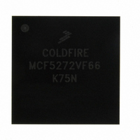
MCF5272VF66 Freescale Semiconductor, MCF5272VF66 Datasheet - Page 204

MCF5272VF66
Manufacturer Part Number
MCF5272VF66
Description
IC MPU 32BIT 66MHZ 196-MAPBGA
Manufacturer
Freescale Semiconductor
Series
MCF527xr
Specifications of MCF5272VF66
Core Processor
Coldfire V2
Core Size
32-Bit
Speed
66MHz
Connectivity
EBI/EMI, Ethernet, I²C, SPI, UART/USART, USB
Peripherals
DMA, WDT
Number Of I /o
32
Program Memory Size
16KB (4K x 32)
Program Memory Type
ROM
Ram Size
1K x 32
Voltage - Supply (vcc/vdd)
3 V ~ 3.6 V
Oscillator Type
External
Operating Temperature
0°C ~ 70°C
Package / Case
196-MAPBGA
Lead Free Status / RoHS Status
Contains lead / RoHS non-compliant
Eeprom Size
-
Data Converters
-
Available stocks
Company
Part Number
Manufacturer
Quantity
Price
Company:
Part Number:
MCF5272VF66
Manufacturer:
HYNIX
Quantity:
19
Company:
Part Number:
MCF5272VF66
Manufacturer:
FREESCAL
Quantity:
885
Company:
Part Number:
MCF5272VF66
Manufacturer:
Freescale Semiconductor
Quantity:
10 000
Part Number:
MCF5272VF66
Manufacturer:
FREESCALE
Quantity:
20 000
Company:
Part Number:
MCF5272VF66J
Manufacturer:
Freescale
Quantity:
256
Company:
Part Number:
MCF5272VF66J
Manufacturer:
Freescale Semiconductor
Quantity:
10 000
Company:
Part Number:
MCF5272VF66R2
Manufacturer:
Freescale Semiconductor
Quantity:
10 000
Company:
Part Number:
MCF5272VF66R2J
Manufacturer:
Freescale Semiconductor
Quantity:
10 000
- Current page: 204 of 544
- Download datasheet (7Mb)
SDRAM Controller
Selecting a system clock frequency low enough that the SDCLK-to-CLK delay is long compared to the
SDRAM read access time reduces effective CAS latency by 1 cycle.
9.10
Setting CSBRn[EBI] to 0b01 enables chip select CS7 for use with one physical bank of SDRAM. In this
case, CS7 becomes SDCS. The SDRAM memory array may have a 32- or 16-bit data bus width; an 8-bit
width is not supported. An array may consist of SDRAM devices with 8, 16, or 32 bits data bus width.
Each SDRAM device can have from 16–256 Mbits.
The interface to the SDRAM devices is glueless. The following control signals are dedicated to SDRAM:
SDCS, SDWE, A10_PRECHG, SDCLK, SDCLKE, RAS0, CAS0, and SDBA[1:0].
If SDRAM EBI mode is used, CSOR7[WAITST] should be programmed for 0x1F to ensure that the
internal bus cycle termination signal is sourced from the SDRAM controller and not the chip select
module.
9-14
Internal CLK
SDRAM Interface
SDCLK
Data
When reduced effective CAS latency is used, the SDRAM is still
programmed with true CAS latency. The SDRAM controller state machine
must be reprogrammed for the reduced CAS latency. SDRAM initialization
software programs the CAS latency of 2 and transfers it into the SDRAM
mode register. After SDRAM initialization is confirmed, initialization
software should change SDTR[CLT] to CAS latency 1 but should not
reinitialize the SDRAM. The SDRAM controller state machine now runs
with CAS latency 1 and SDRAMs run with CAS latency 2, which increases
bandwidth on the SDRAM bank and improves performance.
MCF5272 ColdFire
Figure 9-8. Timing Refinement with Effective CAS Latency
T
SDCLK_to_CLK
Shifted delay of SDCLK
®
Integrated Microprocessor User’s Manual, Rev. 3
- T
CASL = 1
acc
NOTE
> 0 => effective CAS latency reduced by 1
SDRAM read access time
Delay SDCLK to CLK
Freescale Semiconductor
Related parts for MCF5272VF66
Image
Part Number
Description
Manufacturer
Datasheet
Request
R
Part Number:
Description:
Mcf5272 Coldfire Integrated Microprocessor User
Manufacturer:
Freescale Semiconductor, Inc
Datasheet:

Part Number:
Description:
MCF5272 Interrupt Service Routine for the Physical Layer Interface Controller
Manufacturer:
Freescale Semiconductor / Motorola
Datasheet:
Part Number:
Description:
Manufacturer:
Freescale Semiconductor, Inc
Datasheet:
Part Number:
Description:
Manufacturer:
Freescale Semiconductor, Inc
Datasheet:
Part Number:
Description:
Manufacturer:
Freescale Semiconductor, Inc
Datasheet:
Part Number:
Description:
Manufacturer:
Freescale Semiconductor, Inc
Datasheet:
Part Number:
Description:
Manufacturer:
Freescale Semiconductor, Inc
Datasheet:
Part Number:
Description:
Manufacturer:
Freescale Semiconductor, Inc
Datasheet:
Part Number:
Description:
Manufacturer:
Freescale Semiconductor, Inc
Datasheet:
Part Number:
Description:
Manufacturer:
Freescale Semiconductor, Inc
Datasheet:
Part Number:
Description:
Manufacturer:
Freescale Semiconductor, Inc
Datasheet:
Part Number:
Description:
Manufacturer:
Freescale Semiconductor, Inc
Datasheet:
Part Number:
Description:
Manufacturer:
Freescale Semiconductor, Inc
Datasheet:
Part Number:
Description:
Manufacturer:
Freescale Semiconductor, Inc
Datasheet:
Part Number:
Description:
Manufacturer:
Freescale Semiconductor, Inc
Datasheet:


