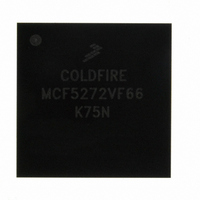
MCF5272VF66 Freescale Semiconductor, MCF5272VF66 Datasheet - Page 489

MCF5272VF66
Manufacturer Part Number
MCF5272VF66
Description
IC MPU 32BIT 66MHZ 196-MAPBGA
Manufacturer
Freescale Semiconductor
Series
MCF527xr
Specifications of MCF5272VF66
Core Processor
Coldfire V2
Core Size
32-Bit
Speed
66MHz
Connectivity
EBI/EMI, Ethernet, I²C, SPI, UART/USART, USB
Peripherals
DMA, WDT
Number Of I /o
32
Program Memory Size
16KB (4K x 32)
Program Memory Type
ROM
Ram Size
1K x 32
Voltage - Supply (vcc/vdd)
3 V ~ 3.6 V
Oscillator Type
External
Operating Temperature
0°C ~ 70°C
Package / Case
196-MAPBGA
Lead Free Status / RoHS Status
Contains lead / RoHS non-compliant
Eeprom Size
-
Data Converters
-
Available stocks
Company
Part Number
Manufacturer
Quantity
Price
Company:
Part Number:
MCF5272VF66
Manufacturer:
HYNIX
Quantity:
19
Company:
Part Number:
MCF5272VF66
Manufacturer:
FREESCAL
Quantity:
885
Company:
Part Number:
MCF5272VF66
Manufacturer:
Freescale Semiconductor
Quantity:
10 000
Part Number:
MCF5272VF66
Manufacturer:
FREESCALE
Quantity:
20 000
Company:
Part Number:
MCF5272VF66J
Manufacturer:
Freescale
Quantity:
256
Company:
Part Number:
MCF5272VF66J
Manufacturer:
Freescale Semiconductor
Quantity:
10 000
Company:
Part Number:
MCF5272VF66R2
Manufacturer:
Freescale Semiconductor
Quantity:
10 000
Company:
Part Number:
MCF5272VF66R2J
Manufacturer:
Freescale Semiconductor
Quantity:
10 000
- Current page: 489 of 544
- Download datasheet (7Mb)
23.3
23.3.1
Table 23-6
1
2
3
Clock input and output timings listed in
Freescale Semiconductor
C1
C2
C3
C4
C4a
C4b
The clock period is referred to as T in the electrical specifications. The time for T is always in nS. Timing specifications can be
given in terms of T. For example, 2T+5 nS
Specification values are not tested.
Specification values listed are for maximum frequency of operation.
2
2
Name
3
3
AC Electrical Specifications
lists clock input and output timings.
Frequency of operation
CLKIN period (T)
CLKIN fall time (from V
CLKIN rise time (from V
CLKIN duty cycle (measured at 1.5 V)
CLKIN pulse-width high (measured at 1.5 V)
CLKIN pulse-width low (measured at 1.5 V)
Clock Input and Output Timing Specifications
AC timing specifications may be subject to change during ongoing
qualification.
AC timing specifications assume maximum output load capacitance on all
output pins including SDCLK. If this value is different, the input and output
timing specifications would need to be adjusted to match the clock load.
AC timing specifications referenced to SDCLK assume SDRAM control
register bit 3 is 0. After reset this bit is set.
CLKIN
(input)
MCF5272 ColdFire
Table 23-6. Clock Input and Output Timing Specifications
1
C4a
h
l
= 2.4 V to V
Figure 23-1. Clock Input Timing Diagram
= 0.5 V to V
Characteristic
®
Integrated Microprocessor User’s Manual, Rev. 3
Table 23-6
l
h
C1
= 0.5 V)
= 2.4 V)
NOTE
are shown in
Figure
C2
23-1.
C4b
6.75
6.75
Min
15
45
—
—
0
V
V
0–66 MHz
h
l
Electrical Characteristics
66.00
Max
8.25
8.25
55
—
2
2
C3
MHz
Unit
nS
nS
nS
nS
nS
%
23-5
Related parts for MCF5272VF66
Image
Part Number
Description
Manufacturer
Datasheet
Request
R
Part Number:
Description:
Mcf5272 Coldfire Integrated Microprocessor User
Manufacturer:
Freescale Semiconductor, Inc
Datasheet:

Part Number:
Description:
MCF5272 Interrupt Service Routine for the Physical Layer Interface Controller
Manufacturer:
Freescale Semiconductor / Motorola
Datasheet:
Part Number:
Description:
Manufacturer:
Freescale Semiconductor, Inc
Datasheet:
Part Number:
Description:
Manufacturer:
Freescale Semiconductor, Inc
Datasheet:
Part Number:
Description:
Manufacturer:
Freescale Semiconductor, Inc
Datasheet:
Part Number:
Description:
Manufacturer:
Freescale Semiconductor, Inc
Datasheet:
Part Number:
Description:
Manufacturer:
Freescale Semiconductor, Inc
Datasheet:
Part Number:
Description:
Manufacturer:
Freescale Semiconductor, Inc
Datasheet:
Part Number:
Description:
Manufacturer:
Freescale Semiconductor, Inc
Datasheet:
Part Number:
Description:
Manufacturer:
Freescale Semiconductor, Inc
Datasheet:
Part Number:
Description:
Manufacturer:
Freescale Semiconductor, Inc
Datasheet:
Part Number:
Description:
Manufacturer:
Freescale Semiconductor, Inc
Datasheet:
Part Number:
Description:
Manufacturer:
Freescale Semiconductor, Inc
Datasheet:
Part Number:
Description:
Manufacturer:
Freescale Semiconductor, Inc
Datasheet:
Part Number:
Description:
Manufacturer:
Freescale Semiconductor, Inc
Datasheet:


