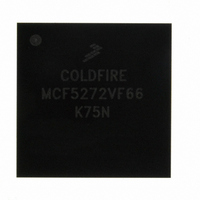
MCF5272VF66 Freescale Semiconductor, MCF5272VF66 Datasheet - Page 510

MCF5272VF66
Manufacturer Part Number
MCF5272VF66
Description
IC MPU 32BIT 66MHZ 196-MAPBGA
Manufacturer
Freescale Semiconductor
Series
MCF527xr
Specifications of MCF5272VF66
Core Processor
Coldfire V2
Core Size
32-Bit
Speed
66MHz
Connectivity
EBI/EMI, Ethernet, I²C, SPI, UART/USART, USB
Peripherals
DMA, WDT
Number Of I /o
32
Program Memory Size
16KB (4K x 32)
Program Memory Type
ROM
Ram Size
1K x 32
Voltage - Supply (vcc/vdd)
3 V ~ 3.6 V
Oscillator Type
External
Operating Temperature
0°C ~ 70°C
Package / Case
196-MAPBGA
Lead Free Status / RoHS Status
Contains lead / RoHS non-compliant
Eeprom Size
-
Data Converters
-
Available stocks
Company
Part Number
Manufacturer
Quantity
Price
Company:
Part Number:
MCF5272VF66
Manufacturer:
HYNIX
Quantity:
19
Company:
Part Number:
MCF5272VF66
Manufacturer:
FREESCAL
Quantity:
885
Company:
Part Number:
MCF5272VF66
Manufacturer:
Freescale Semiconductor
Quantity:
10 000
Part Number:
MCF5272VF66
Manufacturer:
FREESCALE
Quantity:
20 000
Company:
Part Number:
MCF5272VF66J
Manufacturer:
Freescale
Quantity:
256
Company:
Part Number:
MCF5272VF66J
Manufacturer:
Freescale Semiconductor
Quantity:
10 000
Company:
Part Number:
MCF5272VF66R2
Manufacturer:
Freescale Semiconductor
Quantity:
10 000
Company:
Part Number:
MCF5272VF66R2J
Manufacturer:
Freescale Semiconductor
Quantity:
10 000
- Current page: 510 of 544
- Download datasheet (7Mb)
Electrical Characteristics
Figure 23-19
Table 23-20
1
2
3
4
23-26
P52
P53
P54
Name
P50
P51
P57
P58
P59
P60
P61
For most telecommunications applications the period of DFSC[1:3] should be set to 125 µS. Refer to clock generator planning
in PLIC chapter.
GDCL1_OUT must be less than 1/20th of the CPU operating frequency to ensure minimum jitter to CODECs connected to
Ports 1, 2, 3.
Same as DCL0 and FSC0 if internal clock generator configured for pass-through mode.
Based on generated GDCL1_OUT less than 1/20 of CPU clock frequency.
2,4
2,4
2,3
1
1
DOUT[0,1,3]
Delay from rising edge of GDCL1_OUT to rising edge of DFSC[1:3]
Delay from rising edge of GDCL1_OUT to falling edge of DFSC[1:3]
GDCL1_OUT clock period
GDCL1_OUT pulse-width low
GDCL1_OUT pulse-width high
Delay from rising edge of GDCL1_OUT to Low-Z and valid data on DOUT[1,3]
Delay from rising edge of GDCL1_OUT to data valid on DOUT[1,3]
Delay from rising edge of GDCL1_OUT to High-Z on DOUT[1,3]
Data valid on DIN[1:3] before rising edge of GDCL1_OUT (setup time)
Data valid on DIN[1:3] after rising edge of GDCL1_OUT (hold time)
DFSC[2,3]
DIN[0,1,3]
DCL[0:1]
FSC[0,1]
lists timings for GCI master mode.
shows GCI slave timings listed in
MCF5272 ColdFire
P30
Table 23-20. GCI Master Mode Timing, PLIC PORTs 1, 2, 3
P38
P41
P32
P42
Figure 23-19. GCI Slave Mode Timing
Characteristic
®
Integrated Microprocessor User’s Manual, Rev. 3
P31
Table
23-19.
P39
20T
Min
45
45
25
25
—
—
—
—
—
P34
P40
Max
50
50
—
—
—
—
—
—
—
—
Freescale Semiconductor
P33
Unit
20
20
55
55
30
30
30
—
—
—
P35
% of period
% of period
Name
nS
nS
nS
nS
nS
nS
nS
nS
Related parts for MCF5272VF66
Image
Part Number
Description
Manufacturer
Datasheet
Request
R
Part Number:
Description:
Mcf5272 Coldfire Integrated Microprocessor User
Manufacturer:
Freescale Semiconductor, Inc
Datasheet:

Part Number:
Description:
MCF5272 Interrupt Service Routine for the Physical Layer Interface Controller
Manufacturer:
Freescale Semiconductor / Motorola
Datasheet:
Part Number:
Description:
Manufacturer:
Freescale Semiconductor, Inc
Datasheet:
Part Number:
Description:
Manufacturer:
Freescale Semiconductor, Inc
Datasheet:
Part Number:
Description:
Manufacturer:
Freescale Semiconductor, Inc
Datasheet:
Part Number:
Description:
Manufacturer:
Freescale Semiconductor, Inc
Datasheet:
Part Number:
Description:
Manufacturer:
Freescale Semiconductor, Inc
Datasheet:
Part Number:
Description:
Manufacturer:
Freescale Semiconductor, Inc
Datasheet:
Part Number:
Description:
Manufacturer:
Freescale Semiconductor, Inc
Datasheet:
Part Number:
Description:
Manufacturer:
Freescale Semiconductor, Inc
Datasheet:
Part Number:
Description:
Manufacturer:
Freescale Semiconductor, Inc
Datasheet:
Part Number:
Description:
Manufacturer:
Freescale Semiconductor, Inc
Datasheet:
Part Number:
Description:
Manufacturer:
Freescale Semiconductor, Inc
Datasheet:
Part Number:
Description:
Manufacturer:
Freescale Semiconductor, Inc
Datasheet:
Part Number:
Description:
Manufacturer:
Freescale Semiconductor, Inc
Datasheet:


