MCF5272VF66 Freescale Semiconductor, MCF5272VF66 Datasheet - Page 443
MCF5272VF66
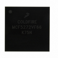
Manufacturer Part Number
MCF5272VF66
Description
IC MPU 32BIT 66MHZ 196-MAPBGA
Manufacturer
Freescale Semiconductor
Series
MCF527xr
Specifications of MCF5272VF66
Core Processor
Coldfire V2
Core Size
32-Bit
Speed
66MHz
Connectivity
EBI/EMI, Ethernet, I²C, SPI, UART/USART, USB
Peripherals
DMA, WDT
Number Of I /o
32
Program Memory Size
16KB (4K x 32)
Program Memory Type
ROM
Ram Size
1K x 32
Voltage - Supply (vcc/vdd)
3 V ~ 3.6 V
Oscillator Type
External
Operating Temperature
0°C ~ 70°C
Package / Case
196-MAPBGA
Lead Free Status / RoHS Status
Contains lead / RoHS non-compliant
Eeprom Size
-
Data Converters
-
Available stocks
Company
Part Number
Manufacturer
Quantity
Price
Company:

Part Number:
MCF5272VF66
Manufacturer:
HYNIX
Quantity:
19
Company:
Part Number:
MCF5272VF66
Manufacturer:
FREESCAL
Quantity:
885
Company:
Part Number:
MCF5272VF66
Manufacturer:
Freescale Semiconductor
Quantity:
10 000
Part Number:
MCF5272VF66
Manufacturer:
FREESCALE
Quantity:
20 000
Company:
Part Number:
MCF5272VF66J
Manufacturer:
Freescale
Quantity:
256
Company:
Part Number:
MCF5272VF66J
Manufacturer:
Freescale Semiconductor
Quantity:
10 000
Company:
Part Number:
MCF5272VF66R2
Manufacturer:
Freescale Semiconductor
Quantity:
10 000
Company:
Part Number:
MCF5272VF66R2J
Manufacturer:
Freescale Semiconductor
Quantity:
10 000


Signal Descriptions
GCI mode: GDCL1_OUT is used to clock data in and out of DIN1 and DOUT1 for GCI port 1. DCL1 is
twice the bit rate; that is, two clocks per data bit.
When this pin is configured as an output, the GDCL1_OUT clock signal from the on-chip synthesizer
clock generator is output on this pin. Also GDCL1_OUT is used to internally drive all ports and delayed
sync generators associated with ports 1, 2, and 3.
19.16.2.2 GCI/IDL Data Out (DOUT1)
IDL mode: The DOUT1 output is for clocking data out of IDL port 1. Data is clocked out of DOUT1 on
the rising edge of DCL1. DOUT1 is also used for clocking data from ports 2 and 3.
GCI mode: The DOUT1 output is for clocking data out of GCI port 1. DCL1 is twice the bit rate, that is,
two clocks per data bit.
19.16.2.3 GCI/IDL Data In (DIN1)
IDL mode: The DIN1 input is for clocking data into IDL port 1. Data is clocked into DIN1 on the falling
edge of DCL1. DIN1 is also used for clocking data into ports 2 and 3.
GCI mode: The DIN1 input is for clocking data into GCI port 1. DCL1 is twice the bit rate, that is, two
clocks per data bit. DIN1 is also used for clocking data into ports 2 and 3.
19.16.2.4 GCI/IDL Frame Sync (FSC1/FSR1/DFSC1)
IDL mode: FSR1 is an input for the 8-KHz frame sync for port 1.
GCI mode: FSC1 is an input for the 8-KHz frame sync for port 1. Normally the GCI FSC signal is two
clocks wide and is aligned with the first B channel bit of the GCI frame. Many U-interface devices
including the MC145572 and MC145576 change the width of FSC to one clock every 12 mS, indicating
a U-interface super frame boundary. The MCF5272 can accept either frame sync width.
When this pin is configured as an output, the DFSC1 sync signal from the on-chip clock synthesizer is
output on this pin. Also DFSC1 is used to internally drive the port 1 frame sync and the delayed sync
generators associated with ports 2 and 3. The width of DFSC1 can be configured for 1, 2, 8, or 16 DCL
clocks duration. The location of DFSC1 is programmable in single clock increments up to a maximum
count of 0x3FF.
19.16.2.5 D-Channel Request (DREQ1/PA14)
IDL mode: This pin can be configured as the DREQ1 output in IDL mode for signalling to a layer 1 S/T
transceiver that a frame of data is ready to be sent on the port 1 D channel.
Port A mode: I/O pin PA14.
19.16.2.6 D-Channel Grant (DGNT1_INT6/PA15_INT6)
This pin can be independently configured as the input, DGNT1, used by a Layer one ISDN S/T transceiver
to indicate that D-channel access has been granted.
®
MCF5272 ColdFire
Integrated Microprocessor User’s Manual, Rev. 3
Freescale Semiconductor
19-33
Related parts for MCF5272VF66
Image
Part Number
Description
Manufacturer
Datasheet
Request
R

Part Number:
Description:
Mcf5272 Coldfire Integrated Microprocessor User
Manufacturer:
Freescale Semiconductor, Inc
Datasheet:

Part Number:
Description:
MCF5272 Interrupt Service Routine for the Physical Layer Interface Controller
Manufacturer:
Freescale Semiconductor / Motorola
Datasheet:
Part Number:
Description:
Manufacturer:
Freescale Semiconductor, Inc
Datasheet:
Part Number:
Description:
Manufacturer:
Freescale Semiconductor, Inc
Datasheet:
Part Number:
Description:
Manufacturer:
Freescale Semiconductor, Inc
Datasheet:
Part Number:
Description:
Manufacturer:
Freescale Semiconductor, Inc
Datasheet:
Part Number:
Description:
Manufacturer:
Freescale Semiconductor, Inc
Datasheet:
Part Number:
Description:
Manufacturer:
Freescale Semiconductor, Inc
Datasheet:
Part Number:
Description:
Manufacturer:
Freescale Semiconductor, Inc
Datasheet:
Part Number:
Description:
Manufacturer:
Freescale Semiconductor, Inc
Datasheet:
Part Number:
Description:
Manufacturer:
Freescale Semiconductor, Inc
Datasheet:
Part Number:
Description:
Manufacturer:
Freescale Semiconductor, Inc
Datasheet:
Part Number:
Description:
Manufacturer:
Freescale Semiconductor, Inc
Datasheet:
Part Number:
Description:
Manufacturer:
Freescale Semiconductor, Inc
Datasheet:
Part Number:
Description:
Manufacturer:
Freescale Semiconductor, Inc
Datasheet: