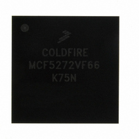
MCF5272VF66 Freescale Semiconductor, MCF5272VF66 Datasheet - Page 446

MCF5272VF66
Manufacturer Part Number
MCF5272VF66
Description
IC MPU 32BIT 66MHZ 196-MAPBGA
Manufacturer
Freescale Semiconductor
Series
MCF527xr
Specifications of MCF5272VF66
Core Processor
Coldfire V2
Core Size
32-Bit
Speed
66MHz
Connectivity
EBI/EMI, Ethernet, I²C, SPI, UART/USART, USB
Peripherals
DMA, WDT
Number Of I /o
32
Program Memory Size
16KB (4K x 32)
Program Memory Type
ROM
Ram Size
1K x 32
Voltage - Supply (vcc/vdd)
3 V ~ 3.6 V
Oscillator Type
External
Operating Temperature
0°C ~ 70°C
Package / Case
196-MAPBGA
Lead Free Status / RoHS Status
Contains lead / RoHS non-compliant
Eeprom Size
-
Data Converters
-
Available stocks
Company
Part Number
Manufacturer
Quantity
Price
Company:
Part Number:
MCF5272VF66
Manufacturer:
HYNIX
Quantity:
19
Company:
Part Number:
MCF5272VF66
Manufacturer:
FREESCAL
Quantity:
885
Company:
Part Number:
MCF5272VF66
Manufacturer:
Freescale Semiconductor
Quantity:
10 000
Part Number:
MCF5272VF66
Manufacturer:
FREESCALE
Quantity:
20 000
Company:
Part Number:
MCF5272VF66J
Manufacturer:
Freescale
Quantity:
256
Company:
Part Number:
MCF5272VF66J
Manufacturer:
Freescale Semiconductor
Quantity:
10 000
Company:
Part Number:
MCF5272VF66R2
Manufacturer:
Freescale Semiconductor
Quantity:
10 000
Company:
Part Number:
MCF5272VF66R2J
Manufacturer:
Freescale Semiconductor
Quantity:
10 000
- Current page: 446 of 544
- Download datasheet (7Mb)
Signal Descriptions
19.17.3 Test and Debug Data Out (TDO/DSO)
JTAG mode: The TDO output is for shifting data out of the serial data port logic. Shifting out of data
depends on the state of the JTAG controller state machine and the instructions currently in the instruction
register. This data shift occurs on the falling edge of TCK. When TDO is not outputting data it is placed
in a high-impedance state. TDO can also be three-stated to allow bussed or parallel connections to other
devices having JTAG test access ports.
BDM mode: DSO is the debug data output.
19.17.4 Test and Debug Data In (TDI/DSI)
JTAG mode: The TDI input is for loading the serial data port shift registers (boundary scan registers,
bypass register and instruction register). Shifting in of data depends on the state of the JTAG controller
state machine and the instruction currently in the instruction register. Data is shifted in on the rising edge
of TCK.
BDM mode: DSI is the debug serial data input. This signal requires a 10-K¾ pullup resistor.
19.17.5 JTAG TRST and BDM Data Clock (TRST/DSCLK)
JTAG mode: TRST asynchronously resets the JTAG TAP logic when low.
BDM mode: DSCLK is the BDM serial data clock input. It requires a 10-K¾ pullup resistor.
19.17.6 Freescale Test Mode Select (MTMOD)
MTMOD: When the MTMOD input is low, JTAG mode is enabled. When it is high, BDM mode is
enabled.
19.17.7 Debug Transfer Error Acknowledge (TEA)
An external slave asserts the TEA input to indicate an error condition for the current bus transfer. It is
provided to allow full debug port capability. The assertion of TEA causes the MCF5272 to abort the
current bus cycle. If a 10-K¾ pullup resistor is not connected, external logic must drive TEA high when it
is inactive. TEA has no effect during SDRAM accesses. If high parasitic capacitance occurs on the printed
circuit board, a lower value pullup resistor may be needed.
19.17.8 Processor Status Outputs (PST[3:0])
PST[3:0] outputs indicate core status, as shown in
Table
19-7. Debug mode timing is synchronous with
the processor clock; status is unrelated to the current bus transfer.
®
MCF5272 ColdFire
Integrated Microprocessor User’s Manual, Rev. 3
19-36
Freescale Semiconductor
Related parts for MCF5272VF66
Image
Part Number
Description
Manufacturer
Datasheet
Request
R
Part Number:
Description:
Mcf5272 Coldfire Integrated Microprocessor User
Manufacturer:
Freescale Semiconductor, Inc
Datasheet:

Part Number:
Description:
MCF5272 Interrupt Service Routine for the Physical Layer Interface Controller
Manufacturer:
Freescale Semiconductor / Motorola
Datasheet:
Part Number:
Description:
Manufacturer:
Freescale Semiconductor, Inc
Datasheet:
Part Number:
Description:
Manufacturer:
Freescale Semiconductor, Inc
Datasheet:
Part Number:
Description:
Manufacturer:
Freescale Semiconductor, Inc
Datasheet:
Part Number:
Description:
Manufacturer:
Freescale Semiconductor, Inc
Datasheet:
Part Number:
Description:
Manufacturer:
Freescale Semiconductor, Inc
Datasheet:
Part Number:
Description:
Manufacturer:
Freescale Semiconductor, Inc
Datasheet:
Part Number:
Description:
Manufacturer:
Freescale Semiconductor, Inc
Datasheet:
Part Number:
Description:
Manufacturer:
Freescale Semiconductor, Inc
Datasheet:
Part Number:
Description:
Manufacturer:
Freescale Semiconductor, Inc
Datasheet:
Part Number:
Description:
Manufacturer:
Freescale Semiconductor, Inc
Datasheet:
Part Number:
Description:
Manufacturer:
Freescale Semiconductor, Inc
Datasheet:
Part Number:
Description:
Manufacturer:
Freescale Semiconductor, Inc
Datasheet:
Part Number:
Description:
Manufacturer:
Freescale Semiconductor, Inc
Datasheet:


