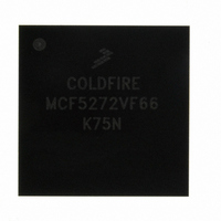
MCF5272VF66 Freescale Semiconductor, MCF5272VF66 Datasheet - Page 430

MCF5272VF66
Manufacturer Part Number
MCF5272VF66
Description
IC MPU 32BIT 66MHZ 196-MAPBGA
Manufacturer
Freescale Semiconductor
Series
MCF527xr
Specifications of MCF5272VF66
Core Processor
Coldfire V2
Core Size
32-Bit
Speed
66MHz
Connectivity
EBI/EMI, Ethernet, I²C, SPI, UART/USART, USB
Peripherals
DMA, WDT
Number Of I /o
32
Program Memory Size
16KB (4K x 32)
Program Memory Type
ROM
Ram Size
1K x 32
Voltage - Supply (vcc/vdd)
3 V ~ 3.6 V
Oscillator Type
External
Operating Temperature
0°C ~ 70°C
Package / Case
196-MAPBGA
Lead Free Status / RoHS Status
Contains lead / RoHS non-compliant
Eeprom Size
-
Data Converters
-
Available stocks
Company
Part Number
Manufacturer
Quantity
Price
Company:
Part Number:
MCF5272VF66
Manufacturer:
HYNIX
Quantity:
19
Company:
Part Number:
MCF5272VF66
Manufacturer:
FREESCAL
Quantity:
885
Company:
Part Number:
MCF5272VF66
Manufacturer:
Freescale Semiconductor
Quantity:
10 000
Part Number:
MCF5272VF66
Manufacturer:
FREESCALE
Quantity:
20 000
Company:
Part Number:
MCF5272VF66J
Manufacturer:
Freescale
Quantity:
256
Company:
Part Number:
MCF5272VF66J
Manufacturer:
Freescale Semiconductor
Quantity:
10 000
Company:
Part Number:
MCF5272VF66R2
Manufacturer:
Freescale Semiconductor
Quantity:
10 000
Company:
Part Number:
MCF5272VF66R2J
Manufacturer:
Freescale Semiconductor
Quantity:
10 000
- Current page: 430 of 544
- Download datasheet (7Mb)
Signal Descriptions
19.6
This section describes bus control signals.
19.6.1
The output enable/read signal (OE/RD) defines the data transfer direction for the data bus D[31:0] for
accesses to SRAM, ROM or external peripherals. A low (logic zero) level indicates a read cycle while a
high (logic one) indicates a write cycle.
This signal is normally connected to the OE pins of external SRAM, ROM, or FLASH.
19.6.2
The byte strobes (BS[3:0]) define the flow of data on the data bus. During SRAM and peripheral accesses,
these outputs indicate that data is to be latched or driven onto a byte of the data when driven low. BSn
signals are asserted only to the memory bytes used during a read or write access.
BSn signals are asserted during accesses to on-chip peripherals but not to on-chip SRAM, cache, or ROM.
During SDRAM accesses, these signals indicate a byte transfer between SDRAM and the MCF5272 when
driven high.
For SRAM or FLASH devices, BS[3:0] outputs should be connected to individual byte strobe signals.
For SDRAM devices, BS[3:0] should be connected to individual SDRAM DQM signals. Note that most
SDRAMs associate DQM3 with the MSB, in which case BS3 should be connected to the SDRAM's
DQM3 input.
19-20
Bus Control Signals
Output Enable/Read (OE/RD)
Byte Strobes (BS[3:0])
BS3 BS2 BS1 BS0
MCF5272 ColdFire
1
1
1
1
0
1
0
0
1
1
1
0
1
0
0
Table 19-3. Byte Strobe Operation for 32-Bit Data Bus
1
1
1
0
1
1
0
0
1
1
0
1
1
0
0
1
1
0
1
1
0
1
0
1
0
1
1
0
1
0
®
1
0
1
1
1
0
1
0
0
1
1
1
0
1
0
Integrated Microprocessor User’s Manual, Rev. 3
FLASH/SRAM
FLASH/SRAM
FLASH/SRAM
FLASH/SRAM
FLASH/SRAM
FLASH/SRAM
FLASH/SRAM
Access Type
SDRAM
SDRAM
SDRAM
SDRAM
SDRAM
SDRAM
SDRAM
None
Access Size Data Located On
Longword
Longword
None
Word
Word
Byte
Byte
D[31:24]
D[23:16]
D[31:16]
D[23:16]
D[31:24]
D[31:16]
D[15:8]
D[15:0]
D[31:0]
D[15:8]
D[15:0]
D[31:0]
D[7:0]
D[7:0]
—
Freescale Semiconductor
Related parts for MCF5272VF66
Image
Part Number
Description
Manufacturer
Datasheet
Request
R
Part Number:
Description:
Mcf5272 Coldfire Integrated Microprocessor User
Manufacturer:
Freescale Semiconductor, Inc
Datasheet:

Part Number:
Description:
MCF5272 Interrupt Service Routine for the Physical Layer Interface Controller
Manufacturer:
Freescale Semiconductor / Motorola
Datasheet:
Part Number:
Description:
Manufacturer:
Freescale Semiconductor, Inc
Datasheet:
Part Number:
Description:
Manufacturer:
Freescale Semiconductor, Inc
Datasheet:
Part Number:
Description:
Manufacturer:
Freescale Semiconductor, Inc
Datasheet:
Part Number:
Description:
Manufacturer:
Freescale Semiconductor, Inc
Datasheet:
Part Number:
Description:
Manufacturer:
Freescale Semiconductor, Inc
Datasheet:
Part Number:
Description:
Manufacturer:
Freescale Semiconductor, Inc
Datasheet:
Part Number:
Description:
Manufacturer:
Freescale Semiconductor, Inc
Datasheet:
Part Number:
Description:
Manufacturer:
Freescale Semiconductor, Inc
Datasheet:
Part Number:
Description:
Manufacturer:
Freescale Semiconductor, Inc
Datasheet:
Part Number:
Description:
Manufacturer:
Freescale Semiconductor, Inc
Datasheet:
Part Number:
Description:
Manufacturer:
Freescale Semiconductor, Inc
Datasheet:
Part Number:
Description:
Manufacturer:
Freescale Semiconductor, Inc
Datasheet:
Part Number:
Description:
Manufacturer:
Freescale Semiconductor, Inc
Datasheet:


