AS3991-BQFT austriamicrosystems, AS3991-BQFT Datasheet
AS3991-BQFT
Specifications of AS3991-BQFT
AS3991-BQFTTR


Related parts for AS3991-BQFT

AS3991-BQFT Summary of contents
Page 1
... FIFO register. To support external MCU and other circuitry a 3.3V regulated supply and clock outputs are available. The regulated supply has 20mA current capability. The AS3990/AS3991 is available in a 64-pin QFN (9mm x 9mm), ensuring the smallest possible footprint. www.austriamicrosystems.com 2 Key Features ...
Page 2
... RFONX 32 Directional RFOPX 33 unit 56 EXT_IN 36 OCSI 37 OSCO 60 VCO www.austriamicrosystems.com 4xC 2xC AS3990/ Regulators AS3991 References Gain IQ Down Filter Conversion Digitizer Mixer Digitizer AFE RF Out RSSI EPC Gen2 Protocol Handling GEN-2 24 Frame Gen Byte FIFO CRC Revision 3.81 38 VDD_D VDD_RF 18 VDD_B 19 Supply ...
Page 3
... AS3990/AS3991 Data Sheet - Contents 1 General Description .............................................................................................................................. 1 2 Key Features ......................................................................................................................................... 1 3 Applications ........................................................................................................................................... 1 4 Pin Assignments ................................................................................................................................... 5 Pin Descriptions ....................................................................................................................................................5 5 Absolute Maximum Ratings .................................................................................................................. 8 6 Electrical Characteristics ....................................................................................................................... 9 7 Detailed Description ............................................................................................................................ 11 Supply .................................................................................................................................................................11 Power Modes .................................................................................................................................................12 Host Communication ..........................................................................................................................................13 VCO and PLL ......................................................................................................................................................13 VCO and External RF Source ........................................................................................................................13 PLL .................................................................................................................................................................13 Chip Status Control ...
Page 4
... AS3990/AS3991 Data Sheet - Idle (80) ..........................................................................................................................................................39 Soft Init (83) ....................................................................................................................................................39 Hop to Main Frequency (84) ..........................................................................................................................39 Hop to Auxiliary Frequency (85) .....................................................................................................................39 Trigger AD Conversion (87) ...........................................................................................................................39 Reset FIFO (8F) .............................................................................................................................................39 Transmission With CRC (90) ..........................................................................................................................39 Transmission With CRC Expecting Header Bit (91) .......................................................................................40 Transmission Without CRC (92) .....................................................................................................................40 Delayed Transmission With CRC (93) ...........................................................................................................40 Delayed Transmission Without CRC (94) ...
Page 5
... INP VSN_MIX 11 SUPI CBIB 12 BID VDD_MIX 13 SUPO www.austriamicrosystems.com AS3990/AS3991 Description Connect de-coupling capacitor to VDD_5LFI DAC output for external amplifier support, Output Resistance of DAC pin is 1kΩ Positive supply for LF input stage, connect to VDD_MIX Substrate Differential mixer positive input Substrate Differential mixer negative input ...
Page 6
... AS3990/AS3991 Data Sheet - Table 1. Pin Descriptions Pin Name Pin Number Pin Type CBV5 14 BID VDD_TXPAB 15 SUPI VEXT 16 SUPI VEXT2 17 SUPI VDD_RF 18 SUPO VDD_B 19 SUPO 1 RFOUTP_1 OUT 20 1 RFOUTP_2 OUT 21 1 VSN_1 SUPI 22 1 VSN_2 SUPI 23 1 VSN_3 SUPI 24 1 VSN_4 SUPI ...
Page 7
... AS3990/AS3991 Data Sheet - Table 1. Pin Descriptions Pin Name Pin Number Pin Type IO6 47 BID IO7 48 BID CLSYS 49 OUT CLK 50 INP VDD_IO 51 SUPI CD2 52 BID CD1 53 BID AGD 54 BID VSN_A 55 SUPI EXT_IN 56 INP VSN_CP 57 SUPI ADC 58 IN VDD_A 59 SUPO VCO 60 INP VOSC ...
Page 8
... AS3990/AS3991 Data Sheet - Absolute Maximum Ratings Stresses beyond those listed in Table 2 and functional operation of the device at these or any other conditions beyond those indicated in Characteristics on page 9 is not implied. Exposure to absolute maximum rating conditions for extended periods may affect device reliability. Table 2. Absolute Maximum Ratings ...
Page 9
... Logic Input/Output - Max. CLK frequency V Input logic low LOW V Input logic high HIGH R Output resistance IO0…IO7 IO R Output resistance CL SYS CL SYS 1. Internal PA is available on AS3991only. www.austriamicrosystems.com Conditions V Consumption EXT V Consumption, EXT2 V = 2.5V EXT2 - All system disabled including supply voltage regulators ...
Page 10
... AS3990/AS3991 Data Sheet - Table 4. Recommended Operating Conditions Symbol Parameter - Supply Voltage Supply voltage (bit vext_low - set) Operating virtual junction T J temperature range T Ambient temperature AMB - Rth junction to exposed die pad www.austriamicrosystems.com Conditions Min - 5.0 - 4.1 - -40 - -40 - Revision 3.81 Typ Max Units 5 ...
Page 11
... AS3990/AS3991 Data Sheet - Detailed Description The RFID reader IC comprises complete analog and digital functionality for reader operation including transmitter and receiver section with complete EPC Gen2 or ISO18000-6C digital protocol support. To integrate as many components as possible, the device also comprises an on-board PLL section with integrated VCO, supply section, DAC and ADC section, and host interface section ...
Page 12
... IC and MCU that are both in the power down mode. If the MCU during 200µs period finds out that the RFID system must react, it confirms the normal mode by setting EN high. Table 5. AS3990/AS3991 Power Modes Power mode Power down Power down SYSCLK of 60kHz Normal power Stand by Listen mode 1. Internal PA is available on AS3991only. www.austriamicrosystems.com (see Table 24). EN OAD2 10k to GND ...
Page 13
... VCO and CP pin valid range is between 0.5V and 2.9V. AS3991 and above have internal VCO set to a frequency range around 1800MHz, later internally divided by two for decreasing the VCO pulling effect. The tuning curve of 1800MHz VCO is divided into 16 segments to decrease VCO gain and attain lowest possible phase noise. Configuration of the 1800MHz VCO tuning range can be manual using option bits vco_r< ...
Page 14
... AS3990/AS3991 Data Sheet - Hopping to the second frequency is triggered, if direct command ‘Hop to auxiliary frequency’ is sent. Hop to the third frequency is similar: the register ‘PLL A/B divider main (16)’ can be written any time the external system has free resources and actual hop is triggered by direct command ‘Hop to main frequency’. ...
Page 15
... AS3990/AS3991 Data Sheet - The two ‘TX length’ registers support in-complete bytes transmission. The high two nibbles in register 1D and the nibble composed of bits ‘TX length byte 2’ (1E) register that should be transmitted. Bit B0 (in register 1E flag that signals the presence of additional bits that do not form a complete byte. The number of bits are stored in bits B1~B3 of the same register (1E). The protocol selection is done by the ‘ ...
Page 16
... AS3990/AS3991 Data Sheet - Table 7. EPC_gen2 - Tari Combinations TARI settings Zero and one length (RT CAL) 640 64 200. 100.00 160 8 213.3 8 256 8 320 8 640 8 40 64/3 533.33 80 64/3 266.67 160 64/3 133.33 213.3 64/3 100.02 256 64/3 320 64/3 640 64/3 Direct Mode Direct mode is applied if the user wants to use analog functions only and bypass the protocol handling supported in the reader IC ...
Page 17
... AS3990/AS3991 Data Sheet - The digital modulation input in direct mode is IO3. RF field is set to high level if IO3 is high, and to low level if IO3 is low. IO2 is used as RX enable. For correct operation, follow the instructions given below: 1. Configuration registers should be defined, starting from reg01 2. Direct command Enable RX (97) should be sent 3 ...
Page 18
... Such system is needed to accommodate the short time used at the highest bit rates in the EPC Gen-2 protocol. 2. Internal PA is available on AS3991only. www.austriamicrosystems.com (see Table 23) ...
Page 19
... AS3990/AS3991 Data Sheet - Gain Gain in the receiving chain can be adjusted to optimize the signal to noise and interference ratio. There are three ways of adjusting: manual adjustment, AGC, and AGL. Manual Adjustment is gain adjustable by setting option bits gain<5:1> in the ‘RX special setting 2 registers’ (0A) (see Table 23) ...
Page 20
... The only case when RX length is not known in advance is reception of the PC+EPC. AS3991 and above handle the afore mentioned issue by using special RX mode. The idea is that reader chip generates an additional interrupt after two bytes (PC part of the PC+EPC field) are received. MCU reads out the two bytes that define the length of the on going telegram and writes it in the RX length register ...
Page 21
... AGD. The 7 LSB gives absolute output level and the MSB Bit is the sign. DA converter is enabled by dac_on bit in the ‘Chip status control’ register (00). Output resistance on DAC pin is 1kΩ typically. For applications that require current, a voltage follower needs to be included. www.austriamicrosystems.com for information on entering direct mode.) ADC Power Interface detector RSSI AS3990/AS3991 Revision 3.81 (see Table ...
Page 22
... AS3990/AS3991 Data Sheet - Converter AD converter intends to support the external power detector placed before or after the circulator to measure actual output power. The analog voltage from the power detector is connected to the ADC pin. AD conversion is triggered by the ‘Trigger AD conversion’ (87) command, and the resulted value is available in the ‘ADC readout register’ (19) Table 38) ...
Page 23
... Regulator and IO control CL_SYS, analog out, and Modulator control (3 bytes deep) PLL main (3 bytes deep) 16 www.austriamicrosystems.com Display microcontroller Optional 8 I/O IRQ CLK CLSYS VCC Tx PA UHF Reader AS3990/AS3991 Rx Optional VCO Register Register Revision 3.81 Length R/W 1 R/W 1 Length R/W 1 R/W 1 R/W ...
Page 24
... AS3990/AS3991 Data Sheet - Table 9. Protocol Sub-setting Registers Adr (hex) PLL auxiliary (3 bytes deep DAC register ADC register 19 Table 10. Status Registers Adr (hex) 0C IRQ and status Interrupt mask register 0D AGC and internal status register 0E RSSI levels 0F AGL status register 10 Table 11. Test Registers ...
Page 25
... AS3990/AS3991 Data Sheet - Table 13. Chip Status Control (00) Bit Signal Name B1 rec_on B0 rf_on 1. Reset EN=L or POR=H Protocol Control (01) – Controls the RFID protocol selection 1 Table 14. Protocol Control (01) Bit Signal Name B7 rx_crc_n B6 dir_mode B5 Prot1 B4 Prot0 B3 RX_cod1 B2 RX_cod0 B1 Tari1 B0 Tari0 1. Preset to 06 (Gen2, Miller2, Tari=25µs) at EN=L or POR=H Control Registers - Low Level Configuration Registers TX Options (02) – ...
Page 26
... AS3990/AS3991 Data Sheet - Options (03) - Gen 2 1 Table 16. RX Options (03) Bit Signal Name B7 Rx_LF3 B6 Rx_LF2 B5 Rx_LF1 B4 Rx_LF0 TRext Preset at por=H or EN=L Gen2: 60 (160kHz) TRcal Low Register (04) – Gen2 1 Table 17. TRcal Low Register (04) Bit Signal Name B7 TRcal7 B6 TRcal6 B5 TRcal5 B4 TRcal4 B3 TRcal3 B2 TRcal2 B1 TRcal1 ...
Page 27
... AS3990/AS3991 Data Sheet - Table 18. TRcal High and Miscellaneous Register (05) Bit Signal Name B4 open_dr B3 TRcal11 B2 TRcal10 B1 TRcal9 B0 TRcal8 1. Preset at por=H or EN=L Gen2: 05 Delayed Transmission Wait Time (06) Table 19. Delayed Transmission Wait Time (06) Bit Signal Name B7 Txdel7 B6 Txdel6 B5 Txdel5 B4 Txdel4 B3 Txdel3 B2 Txdel2 B1 Txdel1 B0 Txdel0 1 ...
Page 28
... AS3990/AS3991 Data Sheet - Wait Time (08) – Defines the time after TX when the RX input is disregarded. 1 Table 21. RX Wait Time (08) Bit Signal Name B7 Rxw7 B6 Rxw6 B5 Rxw5 B4 Rxw4 B3 Rxw3 B2 Rxw2 B1 Rxw1 B0 Rxw0 1. Preset at por=H or EN=L Gen2: 07(44.8µs < 54.25µs…84.5µs – LF:160kHz) ...
Page 29
... B4 etx<4> B3 etx<3> B2 etx<2> B1 etx<1> B0 etx<0> 1. Preset to 02 (Medium driver current) at por=H or EN=L 2. Internal PA is available on AS3991 only. Status Registers IRQ and status register (0C) displays the cause of IRQ and TX/RX status. Table 25. IRQ and Status Register (0C) Bit Signal Name B7 Irq_tx B6 Irg_srx B5 Irq_fifo ...
Page 30
... Bit stream from the Tag has been shorter than expected in the RX length configuration. Such event occurs, for example, if the Tag is not powered sufficiently. When enabled, AS3990/AS3991 will generate an active high Interrupt in case the device detects an error during preamble reception. When enabled, AS3990/AS3991 will generate an active high Interrupt in case no Tag has been answered ...
Page 31
... RFU AGL status (7 steps, 3dB per AS3991: in case r10page<0>=1 (reg12): step) REC_A 001, next silicon automatic sel. vco_r AGL status (7 steps, 3dB per AS3991: in case r10page<0>=1 (reg12): step) REC_B VCO measurement result is presented. Function VCO automatic range select 16 steps result Revision 3 ...
Page 32
... AS3990/AS3991 Data Sheet - Table 30. VCO Status Register (10) Bit Signal Name B3 vco_ri<3> B2 vco_ri<2> B1 vco_ri<1> B0 vco_ri<0> Version Register (13) – Provides the version information. 0x30: AS3990 0x38: AS3991 Test Registers Measurement Selection (11) Table 31. Measurement Selection (11) Bit Signal Name RFU msel<2> B1 msel<1> B0 msel<0> 1. Default: Reset por=H and EN=L Test Setting (12) – ...
Page 33
... Function RFU AS3991: manual VCO range selection AS3991: automatic VCO range enable AS3991: auto range selection speed-up AS3991: auto range selection speed-up AS3991: auto range selection mode AS3991: VCO measurement enable Internal oscillator bias current CL_SYS output frequency Analog mixer DC output on OAD/OAD2 ...
Page 34
... AS3990/AS3991 Data Sheet - Table 33. CL_SYS, Analog Out and CP Control (14) Bit Signal Name 1 cp<1> 0 cp<0> 1. Preset at por=H or EN=L Default setting (Medium VCO bias, CLSYS: 5MHz, min. CP current) Modulator Control Register (15) – (three bytes deep) Table 34. Modulator Control Register (15) Bit Signal Name Analog modulation ...
Page 35
... Function Increase internal PA bias Increase two times 000: 500kHz 001: 250kHz 100: 200kHz PLL reference divider 010: 125kHz (Applies to AS3991 only) 101: 100kHz 110: 50kHz 111: 25kHz Prescaler 32/33, PLL main divider dividing ratio N=B*32+A*33, proposed A/B ratio: 1/3…3 1 ...
Page 36
... AS3990/AS3991 Data Sheet - DAC Control Register (18) 1 Table 37. DAC Control Register (18) Bit Signal Name B7 dac<7> B6 dac<6> B5 dac<5> B4 dac<4> B3 dac<3> B2 dac<2> B1 dac<1> B0 dac<0> 1. Default: reset por=H and EN=L ADC Readout Register (19) Table 38. ADC Readout Register (19) Bit Signal Name B7 adc<7> B6 adc<6> B5 adc<5> B4 adc<4> ...
Page 37
... AS3990/AS3991 Data Sheet - Length 2 (1B) 1 Table 40. RX Length 2 (1B) Bit Signal Name B7 rxl<7> B6 rxl<6> B5 rxl<5> B4 rxl<4> B3 rxl<3> B2 rxl<2> B1 rxl<1> B0 rxl<0> 1. Default: reset por=H, EN=L and at the end of successful reception FIFO Control Registers FIFO status – adr 1C hex number of received bytes and FIFO flags. ...
Page 38
... AS3990/AS3991 Data Sheet - Length Byte2 – adr 1E hex low nibbles of complete bytes, which will be transferred through FIFO and information if there is broken byte and how many bits from it should be transferred. Table 43. TX Length Byte2 - adr 1E hex Bit Signal Name B7 Txl3 B6 Txl2 B5 Txl1 ...
Page 39
... AS3990/AS3991 Data Sheet - Table 44. Command Codes Cmd (hex Description of each direct command is as follows – Idle (80) Command Soft Init (83) This command clears the complete logic and sets the configuration registers to default values. Hop to Main Frequency (84) This command forces the PLL to use frequency setting in ‘PLL A/B divider main register’ ...
Page 40
... AS3990/AS3991 Data Sheet - Transmission With CRC Expecting Header Bit (91) This command functions similar to Transmission with CRC (90), but also informs RX decoding logic that header bit is expected in the response (Gen 2). Transmission Without CRC (92) This command functions similar to Transmission with CRC (90), but CRC is excluded. ...
Page 41
... AS3990/AS3991 Data Sheet - QueryAdjustNic (9B) The QueryAdjustNic command issues the command QueryAdjust followed by two session bits and ‘no change’ parameter. The session bits are taken from ‘TX options’ (02) register. The received RN16 is stored in an internal register for further communication (ACK also achievable from the FIFO. ...
Page 42
... AS3990/AS3991 Data Sheet - Table 45. Pin Assignment in Parallel and Serial Interface Connection and in Case of Direct Mode Parallel normal mode, Pin A/D[0] IO0 IRQ interrupt IRQ 1. SS – Slave Select pin active low 2. MOSI – Master Output, Slave Input 3. MISO – Master Input, Slave Output Communication is initialized by a Start condition, which should be followed by an Address or Command word ...
Page 43
... AS3990/AS3991 Data Sheet - Where: Start = start condition Adr = address with Cont bit low Adrc = address with the Cont bit high Cmd = command byte Data = data byte StopSgl = stop condition for termination of the command or non-continuous address mode StopCont = stop condition for termination of the continuous address mode There are also combinations of different communication modes allowed in a single stream between the start and stop condition ...
Page 44
... AS3990/AS3991 Data Sheet - Figure 6. Parallel Interface Communication with Single Stop Condition “StopSgl” Start condition CLK a1[7] IO7 a1[6:0] d1[6:0] a2[6:0] d2[6:0] IO[6:0] Figure 7. Parallel Interface Communication with Continuous Stop Condition “StopCont” Start condition CLK IO7 a0[7] a0[6:0] d0[6:0] d1[6:0] d2[6:0] d3[6:0] IO[6:0] Figure 8 ...
Page 45
... AS3990/AS3991 Data Sheet - Timing Requirements for Parallel Interface While using parallel interface, there must always be a separation between CLK transitions and IO0…IO7 transitions. Minimum time interval between transition on CLK and data lines is 100ns. Minimum CLK high time interval is 300ns in periods when IO0…IO7 pins are used as data outputs 100ns in periods IO0… ...
Page 46
... AS3990/AS3991 Data Sheet - Timing Diagrams Figure 10. Write Data ENABLE - IO4 t CHD CLK MOSI - IO7 DATAO Figure 11. Read Data ENABLE - IO4 CLK MOSI - IO7 DATAI MISO - IO6 www.austriamicrosystems.com DIS DIH DATAI DATAI DOD DATAI t DOH DATAO ( Revision 3. DATAI t DOD DATAO ( ...
Page 47
... AS3990/AS3991 Data Sheet - Timing Parameters Table 47. Timing Parameters Symbol Parameter General Bit rate BR SDI Clock high time t CH Clock low time t CL Write timing t Data in setup time DIS Data in hold time t DIH t Enable hold time EH Read timing Data out hold time ...
Page 48
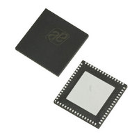
... AS3990/AS3991 Data Sheet - Package Drawings and Markings The device is available in a 64-pin QFN (9mm x 9mm) package. Figure 12. Package Drawings Table 48. Package Dimensions Symbol Min Nom A 0.80 0. 0.203 REF b 0.18 0.23 D 9.00 BSC E 9.00 BSC - REF: Reference Dimension, usually without tolerance, for information purposes only. ...
Page 49
... AS3990/AS3991 Data Sheet - Figure 13. Layout Recommendation According to IPC 7351 Table 49. Layout Dimensions Symbol Distance between two terminals (or leads) on one side from center to Pitch E center positions Width of each terminal land pattern Pad X1 Length of each terminal land pattern Pad Y1 Peripheral terminal (or leads) land pattern length with regard to the ...
Page 50
... AS3990/AS3991 Data Sheet - Ordering Information The devices are available as the standard products shown in Table 50. Ordering Information Model AS3990-BQFW AS3991-BQFW Internal PA, segmented VCO 1. Dry Pack sensitivity Level=3 according to IPC/JEDEC J-STD-033A. www.austriamicrosystems.com Table 50. Description Delivery Form No internal PA Tape and Reel in dry pack Revision 3.81 ...
Page 51
... AS3990/AS3991 Data Sheet - Copyrights Copyright © 1997-2009, austriamicrosystems AG, Schloss Premstaetten, 8141 Unterpremstaetten, Austria-Europe. Trademarks Registered ®. All rights reserved. The material herein may not be reproduced, adapted, merged, translated, stored, or used without the prior written consent of the copyright owner. All products and companies mentioned are trademarks or registered trademarks of their respective companies. ...