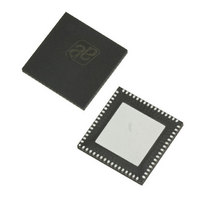
AS3991-BQFT austriamicrosystems, AS3991-BQFT Datasheet - Page 19

AS3991-BQFT
Manufacturer Part Number
AS3991-BQFT
Description
IC UHF RFID READER 64-QFN
Manufacturer
austriamicrosystems
Specifications of AS3991-BQFT
Rf Type
Read / Write
Frequency
840MHz ~ 960MHz
Features
ISO-18000-6
Package / Case
64-VFQFN, Exposed Pad
Lead Free Status / RoHS Status
Lead free / RoHS Compliant
Other names
AS3991-BQFT
AS3991-BQFTTR
AS3991-BQFTTR
AS3990/AS3991
Data Sheet - D e t a i l e d D e s c r i p t i o n
RX Gain
Gain in the receiving chain can be adjusted to optimize the signal to noise and interference ratio. There are three ways
of adjusting: manual adjustment, AGC, and AGL.
Difference between the AGC and AGL functionality is that AGC is done each time at beginning of the receive telegram;
while AGL is done only at the moment when agl_on bit is set high, stored, and is valid till the agl_on bit is set low.
The two receiving signals are digitized and evaluated. The decision circuit selects the in-phase signal or quadrature
signal for further processing, whichever presents the better received signal. Which of the signals is chosen can be
seen in the in_select bit in the ‘AGC and internal status‘ register (0E). Bit is valid from preamble end till start of the next
transmission.
Received Signal Strength Indicator (RSSI)
The receiver section includes a double RSSI meter. The RSSI meters are connected to the outputs of both receiver
chains to measure in real time the peak to peak demodulated voltage of each receiving channel during the reception of
each transponder response (from the end of RX wait timer till the end of reception). The peak value of each RSSI
meter is stored and presented in the ‘RSSI levels’ (0F) register
next transmission.
Reflected RF Level Indicator
The receiver also comprises the input RF level indicator. It is used for diagnostic of circuitry or environment difficulties.
The reflection of poor antenna, reflection of reflective antenna’s environment, or directional device leakage (circulator)
can cause that input mixers are overdriven with the transmitting signal.
Overloading of the input mixers by reflected transmitting carrier can be notified by the host system (MCU) by
measuring the RF input level via internal AD converter. The reflected carrier that is seen on the two mixers input is
down converted to zero frequency. The two DC levels on the mixers outputs are proportional to the input RF level and
dependant on the input phase and can be used for measuring the level of the reflected carrier. They can be connected
to the on-board ADC converter by setting option bits msel<2:0> in the ‘Test setting and measurement selection
register’ (11). The appropriate settings for connecting two mixers’ DC levels to AD converter are 001 and 002.
Conversion is started by direct command ‘Trigger AD conversion’ (87). Result in register 19 is valid 20µs after
triggering.
Normal Mode
In the normal mode, the digitized output after decision circuit is connected to the input of the digital portion of the
receiver. This input signal is the sub-carrier coded signal, which is a digital representation of modulation signal on the
RF carrier.
The digital part of the receiver consists of two sections, which partly overlap. The first section comprises the bit
decoders for the various protocols. The bit decoders convert the sub-carrier coded signal to a bit stream and the data’s
clock according to the protocol defined by option bits Rx-cod<1:0> in the ‘Protocol control’ (01) register
and Rx_LF<3:0> option bits in the ‘RX options’ (03) register. Preamble is truncated. The decoder logic is designed for
maximum error tolerance. This enables the decoders to successfully decode even partly corrupted sub-carrier signals
due to noise or interference. The receiver also supports transfer of incomplete bytes. The number of valid bits in the
last received byte is reported by Bb<2:0> bits in the ‘TX length byte 2’ (1E) register
www.austriamicrosystems.com
Manual Adjustment is gain adjustable by setting option bits gain<5:1> in the ‘RX special setting 2 registers’ (0A)
(see Table
amplifier gain by 3dB (7 steps).
AGC is automatic gain control. It can be enabled by option bit agc_on in the ‘Chip status control’ register (00)
Table
is decreased equally for both channels to a level that results the stronger signal is just in the range. In this case,
the ratio between I and Q channel amplitude is maintained. The resulted status of the AGC can be seen in the
‘AGC and internal status‘ register (0E)
AGL is another possibility for adjusting the gain. AGL bit needs to be set high at the moment when there is no
actual transponder response at receiver input. It automatically decreases gain for each channel to the level that is
just below the noise and interference level. The gain of the two channels is independent. The resulted status of the
AGL for both channels can be seen in the ‘AGL status ‘register (10)
13). AGC comprises of a system that decreases gain during the first periods of the incoming preamble. Gain
23). The low two bits decrease digitizer hysteresis by 5dB (3steps), the high three bits decrease the
(see Table
Revision 3.81
27).
(see Table
(see Table
28). The RSSI register is valid till start of
29).
(see Table
43).
(see Table 14)
19 - 51
(see


