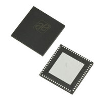
AS3991-BQFT austriamicrosystems, AS3991-BQFT Datasheet - Page 13

AS3991-BQFT
Manufacturer Part Number
AS3991-BQFT
Description
IC UHF RFID READER 64-QFN
Manufacturer
austriamicrosystems
Specifications of AS3991-BQFT
Rf Type
Read / Write
Frequency
840MHz ~ 960MHz
Features
ISO-18000-6
Package / Case
64-VFQFN, Exposed Pad
Lead Free Status / RoHS Status
Lead free / RoHS Compliant
Other names
AS3991-BQFT
AS3991-BQFTTR
AS3991-BQFTTR
AS3990/AS3991
Data Sheet - D e t a i l e d D e s c r i p t i o n
Host Communication
An 8-bit parallel interface (pins IO0 to IO7) with two control signals (CLK, IRQ) forms the main communication system.
It can also be changed (by hardwiring some of the 8 I/O pins) to a serial interface. The data handling is done by a 24
byte FIFO register used in both directions, transmission and reception. For more details, refer
Reader Communication
Interface on page
41.
The signal level for communication between the host system (MCU) is defined by the supply voltage connected to
VDD_IO pin. Communication is possible in wide range between 1.8V and 5.5V. In case the pull-up output resistance at
VDD_IO below 2.7V is to high, it can be decreased by setting option bit vdd_io_low in the ‘TRcal High and Misc
register’ (05). In case the MCU is supplied from the reader IC, then both the MCU supply and VDD_IO pin need to be
connected to VDD_D.
CLSYS output level is defined by the VDD_IO voltage. It is also possible to configure CLSYS to open drain N-MOS
output by setting the option bit open_dr in the in the ‘TRcal high and misc register’ (05),
(see Table
18). This function
can be used to decrease amplitude and harmonic content of the CLSYS signal and decrease the cross-talk effects that
could corrupt operation of other parts of the circuit.
VCO and PLL
The PLL section is composed of a voltage control oscillator (VCO), prescaler, main and reference divider, phase-
frequency detector, charge pump, and loop filter. All building blocks excluding the loop filter are completely integrated.
Operating range is 860MHz to 960MHz.
VCO and External RF Source
Instead of the internal PLL signal, an external RF source can be used. The external source needs to be connected to
EXT_IN pin and option bit eext_in in the ‘PLL A/B divider auxiliary register‘ (17)
(see Table 36)
needs to be set high.
The EXT_IN input optimum level is 0dBm with a DC level between 0V and 2V.
It is also possible to use external VCO and internal PLL circuitry. In this case, the output of the external VCO (0dBm)
needs to be connected to EXT_IN, option bits eext_in and epresc in the ‘PLL A/B divider auxiliary register’ (17) both
need to be set high. The charge pump output pin CP needs to be connected to the external loop filter input and loop
filter output to the external VCO input. This configuration is useful in case the application demands better phase noise
performance than the completely integrated oscillator offers.
The internal on-board VCO is completely integrated including the variable capacitor and inductor. The control input is
pin VCO; input range is between 0 and 3.3V. The option bits eosc<2:0> in the ‘CLSYS, analog out and CP control’ (14)
(Table
33) can be used for oscillator noise and current consumption optimization. Option bit lev_vco in the ‘PLL A/B
divider auxiliary register’ (17)
(see Table 36)
is used to optimize the internal VCO output level to other RF circuitry
demands. VCO and CP pin valid range is between 0.5V and 2.9V.
AS3991 and above have internal VCO set to a frequency range around 1800MHz, later internally divided by two for
decreasing the VCO pulling effect. The tuning curve of 1800MHz VCO is divided into 16 segments to decrease VCO
gain and attain lowest possible phase noise.
Configuration of the 1800MHz VCO tuning range can be manual using option bits vco_r<3:0> in the ‘CL_SYS, analog
out and CP control’ register (14) or automatic using L-H transition on option bit auto in the same register. The device
allows measurement of the VCO voltage using option bit mvco and reading out the 4 bits result of the automatic
segment selection procedure, both in the same register.
PLL
The divide by 32/33 prescaler is controlled by the main divider. The main divider ratio is defined by the ‘PLL A/B divider
main register’ (16). The low ten bits in the three bytes deep register define A value and the next ten bits define B value.
The A and B values define the main divider division ratio to N=B*32+A*33. The reference clock is selectable by
RefFreq<2:0> bits in the ‘PLL R, A/B divider main register’ (16)
(see Table
35). The available values are 500 kHz, 250
kHz, 200 kHz, 100 kHz, 50 kHz, 25 kHz. Charge pump current is selectable between 150µA and 1200µA using option
bits cp1:0 in the ‘CL_SYS, analog out and CP control register’ (14)
(see Table
33). The cp<3> is used to change the
polarity (direction) of the charge pump output.
The frequency hopping is supported by direct commands ‘Hop to main frequency’ (84) and ‘Hop to auxiliary frequency’
(85). The hopping is controlled by host system (MCU) using two configuration registers for two frequencies. Before
enabling the RF field, the host system needs to configure the PLL by writing the ‘CL_SYS, analog out and PLL register’
(09) and the ‘PLL R, A/B divider main’ (16) registers. Any time during operating at the first selected frequency, the
external system can configure the three bytes deep ‘PLL A/B divider auxiliary (17)’ register.
www.austriamicrosystems.com
Revision 3.81
13 - 51


