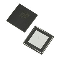
AS3991-BQFT austriamicrosystems, AS3991-BQFT Datasheet - Page 12

AS3991-BQFT
Manufacturer Part Number
AS3991-BQFT
Description
IC UHF RFID READER 64-QFN
Manufacturer
austriamicrosystems
Specifications of AS3991-BQFT
Rf Type
Read / Write
Frequency
840MHz ~ 960MHz
Features
ISO-18000-6
Package / Case
64-VFQFN, Exposed Pad
Lead Free Status / RoHS Status
Lead free / RoHS Compliant
Other names
AS3991-BQFT
AS3991-BQFTTR
AS3991-BQFTTR
AS3990/AS3991
Data Sheet - D e t a i l e d D e s c r i p t i o n
In case lower VEXT supply voltage is used (down to 4.1V), two option bits have to be set to optimize the chip
performance to the lower supply. The vext_low in the ‘TRcal high and misc register’ (05) bit decreases VDD_MIX
voltage to 3.7V to maintain the regulators PSSR and the ir<1> bit in the ‘RX special setting 2’ (0A) adapts mixer’s
internal operating point to lower supply. Adaptation to low supply is implemented in differential mixer only. The
consequence of the decreased supply is lower mixer’s input range.
VDD_5LFI and VDD_TXPAB pins are supply input pins and should be connected to VDD_MIX. The internal 20dBm
power amplifier
the ‘Regulator and IO control register’ (0B)
The input pin is VEXT2 and output is VDD_RF. For optimum noise rejection performance, the input voltage at VEXT2
pin needs to be at least 0.5V above the regulated supply output. Connecting VEXT2 directly to VEXT is possible only
at the expense of increasing IC’s power dissipation and decreasing the maximum operating temperature.
A separate I/O supply pin (VDD_IO) is used to supply the internal level shifters for communication interface to the host
system (MCU). VDD_IO should be connected to MCU supply to ensure proper communication between the chip and
MCU. In case the MCU is supplied by VDD_D from the reader IC also VDD_IO should be connected to VDD_D.
Power Modes
The chip has three power modes.
Power Down with MCU Support mode intends to support the MCU if the majority of the reader IC is in power down.
This mode is enabled by connecting 10kΩ resistor between OAD2 pin and ground. During EN=L period, the VDD_D
regulator is enabled in low power mode and the CLSYS frequency is 60kHz typically.
It is also possible to trigger temporary normal mode from power down mode (EN=L) by pulling shortly the OAD2 pin
low via 10kΩ or less. After the crystal oscillator is stable and the CLSYS clock output is active, the chip waits for
approximately 200µs and then changes back to the power down mode. Using this function, the superior system can
wake up the reader IC and MCU that are both in the power down mode. If the MCU during 200µs period finds out that
the RFID system must react, it confirms the normal mode by setting EN high.
Table 5. AS3990/AS3991 Power Modes
www.austriamicrosystems.com
Power Down Mode: The power down mode is activated by EN pin low (EN=L). For correct operation, the OAD2
pin should not be connected.
Normal Mode: The normal mode is entered by EN=H. In this case all supply regulators, reference voltage system,
crystal oscillator, RF oscillator and PLL are enabled. After the crystal oscillator stabilizes, the CLSYS clock
becomes active (default frequency is 5MHz) and the chip is ready to move to transmit or receive operation.
Standby Mode: The standby mode is entered from normal mode by option bit stby=H. In the standby mode the
regulators, reference voltage system, and crystal oscillator are operating in low power mode; but the PLL,
transmitter output stages and receiver are switched off. All the register settings are kept while switching between
standby and normal mode.
1. Internal PA is available on AS3991only.
SYSCLK of 60kHz
Normal power
Power mode
Power down
Power down
Listen mode
Stand by
1
has an internal regulator from 2…3.5V. The output voltage selection is done by reg2v1:0 option bits in
(see Table
EN
H
L
L
L
-
Revision 3.81
24).
10k and falling edge
10k to GND
OAD2
X
X
-
Std by
X
X
X
H
X
12 - 51


