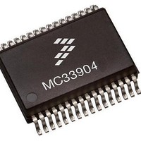
MCZ33904B3EK Freescale Semiconductor, MCZ33904B3EK Datasheet - Page 14

MCZ33904B3EK
Manufacturer Part Number
MCZ33904B3EK
Description
IC SBC CAN HS 3.3V 32SOIC
Manufacturer
Freescale Semiconductor
Type
High Speed CAN Interfacer
Specifications of MCZ33904B3EK
Operating Supply Voltage
3.3 V
Supply Current
2 mA
Package / Case
SOIC-32
Mounting Style
SMD/SMT
Product
CAN
Lead Free Status / RoHS Status
Lead free / RoHS Compliant
Available stocks
Company
Part Number
Manufacturer
Quantity
Price
Company:
Part Number:
MCZ33904B3EKR2
Manufacturer:
FREESCA
Quantity:
4 975
Table 4. 33903/4/5 Pin Definitions (continued)
14
33903/4/5
PIN DEFINITIONS
33905D
54 Pin
24,31
A functional description of each pin can be found in the
10
11
12
13
14
15
16
17
18
19
23
25
8
9
33905S
32 Pin
N/A
N/A
N/A
10
12
13
14
15
16
11
5
6
7
8
9
32 Pin
33904
N/A
N/A
N/A
10
11
12
13
14
15
16
5
6
7
8
9
32 Pin
33903
N/A
N/A
N/A
N/A
N/A
N/A
N/A
10
15
16
5
6
7
8
9
33903D
32 Pin
15, 18
N/A
N/A
N/A
10
12
13
14
16
11
5
6
7
8
9
33903S
32 Pin
15, 18
N/A
N/A
N/A
N/A
N/A
10
11
12
13
5
6
7
8
9
33903P
32 Pin
15, 18
N/A
N/A
N/A
N/A
N/A
10
12
13
11
5
6
7
8
9
GND-CAN
MUX-OUT
Functional Pin Description
Pin Name
5 V-CAN
VCAUX
TXD-L2
RXD-L2
VBAUX
CANH
CANL
SPLIT
VAUX
SAFE
I/O-0
GND
DBG
Function
Ground
Ground
Output
Output
Output
Output
Output
Output
Output
Output
Output
Output
Output
Input/
Input
Input
Pin
(Active LOW)
SPLIT Output Output pin for connection to the
LIN Transmit
OR Auxiliary
Input/Output
Safe Output
VB Auxiliary
LIN Receive
VCOLLECT
GND-CAN
CAN High
CAN Low
Multiplex
Auxiliary
5V-CAN
Formal
Ground
Output
Debug
Data 2
Name
VOUT
Data
0
section beginning on
Analog Integrated Circuit Device Data
Output of the safe circuitry. The pin is
asserted LOW if a fault event occurs
(e.g.: software watchdog is not
triggered, V
pin, etc.). Open drain structure.
Output voltage for the embedded
CAN interface. A capacitor must be
connected to this pin.
CAN high output.
CAN low output.
Power GND of the embedded CAN
interface
middle point of the split CAN
termination
Output pin for external path PNP
transistor base
Output pin for external path PNP
transistor collector
Output pin for the auxiliary voltage.
Multiplexed output to be connected to
an MCU A/D input. Selection of the
analog parameter available at MUX-
OUT is done via the SPI. A
switchable internal pull-down resistor
is integrated for V
measurements.
Configurable pin as an input or
output, for connection to external
circuitry (switched or small load). The
voltage level can be read by the SPI
and via the MUX output pin. The
input can be used as a
programmable Wake-up input in LP
mode. In LP, when used as an
output, the High Side (HS) or Low
Side (LS) can be activated for a cyclic
sense function.
Input to activate the Debug mode. In
Debug mode, no watchdog refresh is
necessary. Outside of Debug mode,
connection of a resistor between
DBG and GND allows the selection of
Safe mode functionality.
LIN bus transmit data input. Includes
an internal pull-up resistor to VDD.
Ground of the IC.
LIN bus receive data output.
Freescale Semiconductor
DD
Definition
page
low, issue on the RST
DD
current sense
35.


