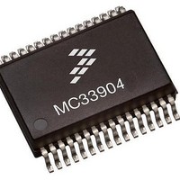
MCZ33904B3EK Freescale Semiconductor, MCZ33904B3EK Datasheet - Page 40

MCZ33904B3EK
Manufacturer Part Number
MCZ33904B3EK
Description
IC SBC CAN HS 3.3V 32SOIC
Manufacturer
Freescale Semiconductor
Type
High Speed CAN Interfacer
Specifications of MCZ33904B3EK
Operating Supply Voltage
3.3 V
Supply Current
2 mA
Package / Case
SOIC-32
Mounting Style
SMD/SMT
Product
CAN
Lead Free Status / RoHS Status
Lead free / RoHS Compliant
Available stocks
Company
Part Number
Manufacturer
Quantity
Price
Company:
Part Number:
MCZ33904B3EKR2
Manufacturer:
FREESCA
Quantity:
4 975
pin, or by the SPI command (Ref. to MODE register).
OFF, and LP mode with V
flags must be cleared (Ref. to mode register). If the Wake-up
flags are not cleared, the device will not enter into LP mode.
In addition, the CAN failure flags (i.e. CAN_F and CAN_UF)
must be cleared, in order to meet the LP current consumption
specification.
LP - V
to VDD is unsupplied. This mode is entered using SPI. It can
also be entered by an automatic transition due to fail-safe
management. 5 V-CAN and V
OFF.
external events to Wake-up and leave the LP mode. The
Wake-up events can occur from:
Reset mode and then into Normal Request mode. The Wake-
up sources are reported to the device SPI registers. In
summary, a Wake-up event from LP V
V
LP - V
(or 3.3 V, depending upon device part number). The
objective is to maintain the MCU powered, with reduced
consumption. In such mode, the DC output current is
expected to be limited to 100 A or a few mA, as the ECU is
in reduced power operation mode.
40
33903/4/5
FUNCTIONAL DEVICE OPERATION
LP MODES
DD
Debug can be left by removing 8 to 10 V from the DEBUG
The device has two main LP modes: LP mode with V
Prior to entering into LP mode, I/O and CAN Wake-up
In this mode, V
When the device is in LP V
• CAN
• LIN interface, depending upon device part number
• Expiration of an internal timer
• I/O-0, and I/O-1 inputs, and depending upon device part
• Cyclic sense of I/O-1 input, associated by I/O-0
When a Wake-up event is detected, the device enters into
In this mode, the voltage at the VDD pin remains at 5.0 V
regulator turned ON, and the MCU operation restart.
number and configuration, I/O-2 and/or -3 input
activation, and depending upon device part number and
configuration, cyclic sense of I/O-2 and -3 input,
associated by I/O-0 activation
DD
DD
OFF
ON
DD
is turned OFF and the MCU connected
DD
ON.
AUX
DD
OFF mode, it monitors
regulators are also turned
DD
OFF leads to the
DD
LP MODES
OFF. The optional external PNP at VDD will also be
automatically disabled when entering this mode.
LIN, I/O, timer, cyclic sense) are available in LP V
mode.
available.
tenths of mA DC. The current source capability can be time
limited, by a selectable internal timer. Timer duration is up to
32 ms, and is triggered when the output current exceed the
output current threshold typically 1.5 mA.
while the device remains in LP V
exceed the selected time (ex 32 ms), the device will detect a
Wake-up.
pulse at INT pulse. The MCU will detect the INT pulse and
resume operation.
Watchdog Function in LP V
ON mode. In this case, the principle is timeout.
remains in LP V
Mode Transitions
timeout expired or voltage conditions), or via a SPI command,
or by an external event such as a Wake-up. Some mode
changes are performed using the Secured SPI commands.
The 5 V-CAN regulator is ON by default in Debug mode.
During this mode, the 5 V-CAN and V
The same Wake-up events as in LP V
In addition, two additional Wake-up conditions are
• Dedicated SPI command. When device is in LP V
• Output current from VDD exceeding L
In LP V
This allows for instance, a periodic activation of the MCU,
Wake-up events are reported to the MCU via a low level
It is possible to enable the watchdog function in LP V
Refresh of the watchdog is done either by:
• a dedicated SPI command (different from any other SPI
• or by a temporary (less than 32 ms max) V
As long as the watchdog refresh occurs, the device
Mode transitions are either done automatically (i.e. after a
mode, the Wake-up by SPI command uses a write to
“Normal Request mode”, 0x5C10.
command or simple CS activation which would Wake-
up - Ref. to the previous paragraph)
current Wake-up (I
DD
ON mode, the device is able to source several
DD
on mode.
Analog Integrated Circuit Device Data
DD
> 1.5 mA typically).
DD
DD
ON Mode
Freescale Semiconductor
on mode. If the duration
DD
AUX
OFF mode (CAN,
P-ITH
regulators are
DD
threshold.
DD
over
on
DD
DD
ON


