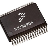
MCZ33904B3EK Freescale Semiconductor, MCZ33904B3EK Datasheet - Page 69

MCZ33904B3EK
Manufacturer Part Number
MCZ33904B3EK
Description
IC SBC CAN HS 3.3V 32SOIC
Manufacturer
Freescale Semiconductor
Type
High Speed CAN Interfacer
Specifications of MCZ33904B3EK
Operating Supply Voltage
3.3 V
Supply Current
2 mA
Package / Case
SOIC-32
Mounting Style
SMD/SMT
Product
CAN
Lead Free Status / RoHS Status
Lead free / RoHS Compliant
Available stocks
Company
Part Number
Manufacturer
Quantity
Price
Company:
Part Number:
MCZ33904B3EKR2
Manufacturer:
FREESCA
Quantity:
4 975
INIT REGISTERS
Analog Integrated Circuit Device Data
Freescale Semiconductor
Table 17. Initialization Regulator Registers, INIT REG (note: register can be written only in INIT mode)
Note: these registers can be written only in INIT mode
[b_15 b_14] 0_0101 [P/N]
b6, b5
b4, b3
b1, b0
MOSI First Byte [15-8]
Bit
Condition for default
b7
00
01
10
11
00
01
10
11
b2
00
01
10
11
0
1
0
1
01 00 _ 101 P
Default state
V
DD RST
D[1] V
I/O-x sync
Cyclic on[1] Cyclic on[0] - Determine I/O-0 activation time, when cyclic sense function is selected
I/O-x sync - Determine if I/O-1 is sensed during I/O-0 activation, when cyclic sense function is selected
bit 7
V
1
DD RST
DDL RST
D[0] - Select the RST pin low lev duration, after V
[1] V
V
DDL
DDL RST
bit 6
1600 s (typical value. Ref. to dynamic parameters for exact value)
200 s (typical value. Ref. to dynamic parameters for exact value)
400 s (typical value. Ref. to dynamic parameters for exact value)
800 s (typical value. Ref. to dynamic parameters for exact value)
0
rst[1]
[0] - Select the V
INT at approx 0.9 V
V
[V
DDL
AUX
bit 5
0
I/O-1 sense during I/O-0 activation
rst[0]
5/3] - Select Vauxilary output voltage
Reset at approx 0.9 V
Reset at approx 0.9 V
Reset at approx 0.7 V
I/O-1 sense anytime
DD
V
Description
under-voltage threshold, to activate RST pin and/or INT
V
V
MOSI Second Byte, bits 7-0
DD
AUX
AUX
DD
bit 4
1.0 ms
5.0 ms
10 ms
20 ms
rstD[1]
0
, Reset at approx 0.7 V
= 3.3 V
= 5.0 V
POR
DETAIL OF CONTROL BITS AND REGISTER MAPPING
V
DD
DD
DD
DD
DD
bit 3
.
.
rstD[0]
0
rises above the V
DD
V
AUX
bit 2
0
SERIAL PERIPHERAL INTERFACE
5/3
DD
under-voltage threshold
Cyclic on[1]
bit 1
0
Cyclic on[0]
bit 0
33903/4/5
0
69


