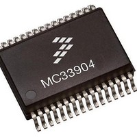
MCZ33904B3EK Freescale Semiconductor, MCZ33904B3EK Datasheet - Page 76

MCZ33904B3EK
Manufacturer Part Number
MCZ33904B3EK
Description
IC SBC CAN HS 3.3V 32SOIC
Manufacturer
Freescale Semiconductor
Type
High Speed CAN Interfacer
Specifications of MCZ33904B3EK
Operating Supply Voltage
3.3 V
Supply Current
2 mA
Package / Case
SOIC-32
Mounting Style
SMD/SMT
Product
CAN
Lead Free Status / RoHS Status
Lead free / RoHS Compliant
Available stocks
Company
Part Number
Manufacturer
Quantity
Price
Company:
Part Number:
MCZ33904B3EKR2
Manufacturer:
FREESCA
Quantity:
4 975
flags must be cleared or read.
39, Device Flag, I/O Real Time and Device
the selected LP mode and immediately Wake-up. In addition,
the CAN failure flags (i.e. CAN_F and CAN_UF) must be
cleared in order to meet the low power current consumption
specification. This is done by the following SPI command:
76
33903/4/5
SERIAL PERIPHERAL INTERFACE
DETAIL OF CONTROL BITS AND REGISTER MAPPING
Table 28. LP V
Table 29. LP V
Prior to enter in LP V
This is done by the following SPI commands (See
0xE100 for CAN Wake-up clear
0xE380 for I/O Wake-up clear
0xE700 for LIN1 Wake-up clear
0xE900 for LIN2 Wake-up clear
If Wake-up flags are not cleared, the device will enter into
0xE180 (read CAN failure flags)
b7, b6, b5, b4, b3
b2, b1, b0
1 0000
1 0001
1 0010
1 0011
1 0100
1 0101
1 0110
1 0111
1 1000
1 1001
1 1010
1 1011
1 1100
1 1101
1 1110
1 1111
DD
DD
OFF Selection and FWU / Cyclic Sense Selection
ON Selection and Operation Mode
DD
b7, b6, b5, b4, b3
ON or LP V
0 1100
0 1101
0 1110
0 1111
Random Code inverted, these 3bits are the inverted bits obtained from the previous SPI command.
The usage of these bits are optional and must be previously selected in the INIT MISC register [See
bit 7 (LPM w RNDM) in
DD
OFF, the Wake-up
Identification):
FWU
OFF
OFF
OFF
OFF
OFF
OFF
OFF
OFF
ON
ON
ON
ON
ON
ON
ON
ON
Table
Table
Cyclic Sense
20]
a SPI command uses a write to “Normal Request mode”,
0x5C10.
Mode Register Features
SPI command” that allow the following:
address bit [13-9], along with several combinations of bit [15-
14] and bit [7]. Note, bit [8] is always set to 1.
OFF
OFF
OFF
OFF
OFF
OFF
OFF
OFF
ON
ON
ON
ON
ON
ON
ON
ON
When the device is in LP V
The mode register includes specific functions and a “global
- read device current mode
- read device Debug status
- read state of SAFE pin
- leave Debug state
- release or turn off SAFE pin
- read a 3 bit Random Code to enter in LP mode
These global commands are built using the MODE register
FWU
OFF
OFF
ON
ON
Cyclic INT
OFF
OFF
OFF
OFF
OFF
OFF
OFF
OFF
Analog Integrated Circuit Device Data
ON
ON
ON
ON
ON
ON
ON
ON
DD
ON mode, the Wake-up by
Freescale Semiconductor
Cyclic Sense
OFF
OFF
ON
ON
Watchdog
OFF
OFF
OFF
OFF
OFF
OFF
OFF
OFF
ON
ON
ON
ON
ON
ON
ON
ON


