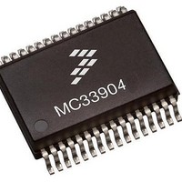
MCZ33904B3EK Freescale Semiconductor, MCZ33904B3EK Datasheet - Page 72

MCZ33904B3EK
Manufacturer Part Number
MCZ33904B3EK
Description
IC SBC CAN HS 3.3V 32SOIC
Manufacturer
Freescale Semiconductor
Type
High Speed CAN Interfacer
Specifications of MCZ33904B3EK
Operating Supply Voltage
3.3 V
Supply Current
2 mA
Package / Case
SOIC-32
Mounting Style
SMD/SMT
Product
CAN
Lead Free Status / RoHS Status
Lead free / RoHS Compliant
Available stocks
Company
Part Number
Manufacturer
Quantity
Price
Company:
Part Number:
MCZ33904B3EKR2
Manufacturer:
FREESCA
Quantity:
4 975
72
33903/4/5
SERIAL PERIPHERAL INTERFACE
DETAIL OF CONTROL BITS AND REGISTER MAPPING
Table 20. Initialization Miscellaneous Functions, INIT MISC (Note: Register can be written only in INIT mode)
Notes
39.
b2, b1, b0
[b_15 b_14] 0_1000 [P/N]
MOSI First Byte [15-8]
100
101
110
111
Bit
0xx
Condition for default
b7
b6
b5
b4
b3
0
1
0
1
0
1
0
1
Bits b2,1 and 0 allow the following operation:
First, check the resistor device has detected at the DEBUG pin. If the resistor is different, bit 5 (Debug resistor) is set in INTerrupt
register (Ref. to device flag table).
Second, over write the resistor decoded by device, to set the SAFE mode operation by SPI. Once this function is selected by bit 2 = 1,
this selection has higher priority than “hardware”, and device will behave according to b2,b1 and b0 setting
01 01_ 000 P
Default state
Dbg Res[2], Dbg Res[1], Dbg Res[0] - Allow verification of the external resistor connected at DBG pin. Ref. to parametric table for resistor range
LPM w RNDM - This enables the usage of random bits 2, 1 and 0 of the MODE register to enter into LP VDD OFF or LP VDD ON.
LPM w RNDM
Function enable: an INT pulse will occur at 50% of the Watchdog Period when device in Flash mode.
100 verification enable: resistor at DBG pin is typically 68 kohm (RB3) - Selection of SAFE mode B3
110 verification enable: resistor at DBG pin is typically 15 kohm (RB1) - Selection of SAFE mode B1
bit 7
101 verification enable: resistor at DBG pin is typically 33 kohm (RB2 - Selection of SAFE mode B2
111 verification enable: resistor at DBG pin is typically 0 kohm (RA) - Selection of SAFE mode A
0
INT pulse duration is typically 100 s. Ref. to dynamic parameter table for exact value.
INT flash - Select INT pulse generation at 50% of the Watchdog Period in Flash mode
INT pulse duration is typically 25 s. Ref. to dynamic parameter table for exact value.
Function disable: the parity is not used. The parity bit must always set to logic 0.
Function disable: the LP mode can be entered without usage of Random Code
SPI parity
bit 6
Function enabled: the LP mode is entered using the Random Code
Function enable: the parity is used, and parity must be calculated.
0
INT pulse -Select INT pin operation: low level pulse or low level
INT pin will assert a low level pulse, duration selected by bit [b4]
SPI parity - Select usage of the parity bit in SPI write operation
INT pin assert a permanent low level (no pulse)
INT pulse
INT width - Select the INT pulse duration
bit 5
0
Function disable
Function disable
Description
INT width
MOSI Second Byte, bits 7-0
value.
bit 4
(39)
POR
INT flash
bit 3
0
Analog Integrated Circuit Device Data
Dbg Res[2]
bit 2
0
Freescale Semiconductor
Dbg Res[1]
bit 1
0
Dbg Res[0]
bit 0
0


