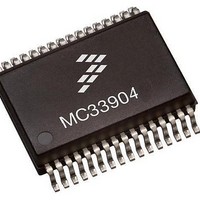
MCZ33904B3EK Freescale Semiconductor, MCZ33904B3EK Datasheet - Page 64

MCZ33904B3EK
Manufacturer Part Number
MCZ33904B3EK
Description
IC SBC CAN HS 3.3V 32SOIC
Manufacturer
Freescale Semiconductor
Type
High Speed CAN Interfacer
Specifications of MCZ33904B3EK
Operating Supply Voltage
3.3 V
Supply Current
2 mA
Package / Case
SOIC-32
Mounting Style
SMD/SMT
Product
CAN
Lead Free Status / RoHS Status
Lead free / RoHS Compliant
Available stocks
Company
Part Number
Manufacturer
Quantity
Price
Company:
Part Number:
MCZ33904B3EKR2
Manufacturer:
FREESCA
Quantity:
4 975
SPI Operation Deviation (does not apply to “C” version)
interpreted by the device. This results in either a “non
received SPI command” or a “corrupted SPI command”.
Important: Due to this, the t
must be carefully acknowledged.
are affected. The SPI read commands (starting with bits
15,14 = 00 or 11) are not affected.
caused by the synchronization between internal and external
signals. In order to guarantee proper operation, the following
steps must be taken.
not specified and is indirectly defined by the sum of 3
parameters, t
parameter is a min of 30 ns.
additional SPI read is necessary. The recommended SPI
read command is “device ID read: 0x2580” so device
operation is not affected (ex: clear flag). Other SPI read
commands may also be used.
BITS 15, 14, AND 8 FUNCTIONS
64
33903/4/5
SERIAL PERIPHERAL INTERFACE
DETAIL OPERATION
Table 12. SPI Operations (bits 8, 14, & 15)
1. Ensure the duration of the Chip Select Low (t
2. Ensure SPI timing parameter t
3. Make sure to include a SPI read command after a
In some cases, the SPI write command is not properly
Only SPI write commands (starting with bits 15,14 = 01)
The occurrence of this issue is extremely low and is
Note: In data sheet revisions prior to 7.0, this parameter is
Note: In data sheet revisions prior to 7.0, the t
In case a series of SPI write commands is used, only one
Table 12
Control Bits MOSI[15-14], C1-C0
state is >5.5 s.
550 ns.
SPI write command.
summarizes the various SPI operation, depending upon bit 15, 14, and 8.
LEAD
00
01
10
11
+ 16 x t
PCLK
LEAD
+ t
and t
LAG
Read back of register
content and block (CAN,
I/O, INT, LINs) real time
state. See
Write to register
address, to control the
device operation
Reserved
Read of device flags
form a register address
LEAD
(sum = 4.06 s).
Type of Command
CSLOW
is a min. of
Table
parameters
LEAD
39.
DETAIL OPERATION
CSLOW
)
MOSI[8] P/N
Parity/Next
1
0
1
1
operate as follows:
• In case the SPI write command ‘n’ is not accepted, the
• By applying steps 1, 2, and 3, no SPI command is ignored.
thanks to step 1 (extension of t
• 0x60C0 (CAN interface control) – in case this command is
• 0x66C0 (LIN interface control) – in case this command is
• 0x2580 (read device ID) – Additional command to
• 0x60C0 (CAN interface control) - in case this command is
• 0x66C0 (LIN interface control) - in case this command is
• 0x2100 (read CAN register content) – this command will
• 0x2700 (read LIN register content)
When the previous steps are implemented, the device will
For a given SPI write command (named SPI write ‘n’):
following SPI command (named SPI ‘n+1’) will finish the
write process of the SPI write ‘n’, thanks to step 2
(t
command ‘n+1’).
Worst case, the SPI write ‘n’ is executed at the time the
SPI ‘n+1’ is sent. This will lead to a delay in device
operation (delay between SPI command ‘n’ and ‘n+1’).
Note: Occurrence of an incorrect command is reduced,
Sequence examples:
Example 1:
missed, next write command will complete it
missed, next read command will complete it
complete previous LIN command, in case it was missed
Example 2:
missed, next write command will complete it
missed, next read command will complete it
complete previous one, in case it was missed
LAG
Bit 8 must be set to 1, independently of the parity function
selected or not selected.
If bit 8 is set to “0”: means parity not selected OR
parity is selected AND parity = 0
if bit 8 is set to “1”: means parity is selected AND parity = 1
Bit 8 must be set to 1, independently of the parity function
selected or not selected.
> 550 ns) and step 3 (which is the additional SPI
Analog Integrated Circuit Device Data
Note for Bit 8 P/N
CSLOW
Freescale Semiconductor
duration to >5.5 s).


