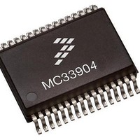
MCZ33904B3EK Freescale Semiconductor, MCZ33904B3EK Datasheet - Page 65

MCZ33904B3EK
Manufacturer Part Number
MCZ33904B3EK
Description
IC SBC CAN HS 3.3V 32SOIC
Manufacturer
Freescale Semiconductor
Type
High Speed CAN Interfacer
Specifications of MCZ33904B3EK
Operating Supply Voltage
3.3 V
Supply Current
2 mA
Package / Case
SOIC-32
Mounting Style
SMD/SMT
Product
CAN
Lead Free Status / RoHS Status
Lead free / RoHS Compliant
Available stocks
Company
Part Number
Manufacturer
Quantity
Price
Company:
Part Number:
MCZ33904B3EKR2
Manufacturer:
FREESCA
Quantity:
4 975
BITS 13-9 FUNCTIONS
(bits 13 to 9).
function. Data can be written to the register to control the
device operation or to set the default value or behavior.
that it’s content (default setting or value previously written) is
correct.
flags.
Table 13. Device Registers with Corresponding Address
Analog Integrated Circuit Device Data
Freescale Semiconductor
The device contains several registers coded on five bits
Each register controls or reports part of the device’s
Every register can also be read back in order to ensure
MOSI[13-9]
In addition, some of the registers are used to report device
Address
A4...A0
0_0000
0_0001
0_0010
0_0011
0_0100
0_0101
0_0110
0_0111
0_1000
0_1001
0_1010
0_1011
0_1100
0_1101
0_1110
0_1111
1_0000
1_0001
1_0010
1_0011
1_0100
Timer_A: watchdog & LP MCU consumption
Timer_C: watchdog LP & Forced Wake-up
Timer_B: Cyclic Sense & Cyclic Interrupt
Initialization Miscellaneous functions
Initialization LIN and I/O
Initialization Regulators
Initialization Watchdog
CAN interface control
LIN2 interface control
LIN1 interface control
Input Output control
Watchdog Refresh
Analog Multiplexer
Regulator Control
Interrupt Control
Memory byte A
Memory byte B
Memory byte C
Memory byte D
Specific modes
Mode register
Description
Init watchdog
SPE_MODE
Quick Ref.
Init LIN I/O
watchdog
Init MISC
Init REG
Interrupt
RAM_A
RAM_B
RAM_C
RAM_D
TIM_A
TIM_B
TIM_C
MODE
Name
MUX
REG
CAN
LIN1
LIN2
I/O
Device Status on MISO
control bits into the device, the MISO pin reports a 16 bit fixed
device status composed of 2 bytes: Device Fixed Status (bits
15 to 8) + extended Device Status (bits 7 to 0). In a read
operation, MISO will report the Fixed device status (bits 15 to
8) and the next eight bits will be the content of the selected
register.
REGISTER ADRESS TABLE
with bits 13 to 9.
When a write operation is performed to store data or
Table 13
1) Write to register to select LP mode, with optional “Inverted Random
1) Write to register to select device Specific mode, using “Inverted
1) Write “device control bits” to register address, to select device
2) Read back “initialization control bits” from register address
1) Write “device initialization control bits” to register address.
3) Read device flags from each of the register addresses.
1) Write “device control bits” to register address.
is a list of device registers and addresses, coded
2) Read back “data byte” from register address
1) Write “timing values” to register address.
1) Write “data byte” to register address.
code” and select Wake-up functionality
2) Read back register “timing values”
2) Read back register “control bits”.
2) Read back register “control bits”
Read back device “Current mode”
Watchdog Refresh Commands
2) Read “Random Code”
Read “Random Code”,
Leave “Debug mode”
2) Read operations:
Random Code”.
Functionality
SERIAL PERIPHERAL INTERFACE
operation.
DETAIL OPERATION
33903/4/5
65


