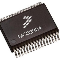
MCZ33904B3EK Freescale Semiconductor, MCZ33904B3EK Datasheet - Page 36

MCZ33904B3EK
Manufacturer Part Number
MCZ33904B3EK
Description
IC SBC CAN HS 3.3V 32SOIC
Manufacturer
Freescale Semiconductor
Type
High Speed CAN Interfacer
Specifications of MCZ33904B3EK
Operating Supply Voltage
3.3 V
Supply Current
2 mA
Package / Case
SOIC-32
Mounting Style
SMD/SMT
Product
CAN
Lead Free Status / RoHS Status
Lead free / RoHS Compliant
Available stocks
Company
Part Number
Manufacturer
Quantity
Price
Company:
Part Number:
MCZ33904B3EKR2
Manufacturer:
FREESCA
Quantity:
4 975
OFF. V
information will disable V
can generate INT.
UNDER-VOLTAGE RESET AND RESET FUNCTION
(RST)
pull-up resistor. The LS driver has limited current capability
when asserted low, in order to tolerate a short to 5.0 V. The
RST pin voltage is monitored in order to detect failure (e.g.
RST pin shorted to 5.0 V or GND).
MCU at the VDD pin, as a RST failure in the watchdog refresh
operation. V
ON mode.
upper (typically 4.65 V, R
Interrupt. This is selected by the SPI. When “R
selected, in Normal mode, an INT is asserted when VDD falls
below “R
Reset will occur. This will allow the MCU to operate in a
degraded mode (i.e., with 4.0 V V
I/O PINS (I/O-0: I/O-3)
for small loads or to drive external transistors. When used as
output drivers, the I/Os are either a HS or LS type. They can
also be set to high-impedance. I/Os are controlled by the SPI
and at power on, the I/Os are set as inputs. They include
over-load protection by temperature or excess of a voltage
drop.
voltage, the leakage current (
applicable
• I/O-0 and I/O-1 will have current flowing into the device
• I/O-2 and I/O-3 will have unlimited current flowing into the
with extremely low power consumption (except when there is
a load). Protection is disabled in LP mode.
36
33903/4/5
FUNCTIONAL DESCRIPTION
FUNCTIONAL PIN DESCRIPTION
V
V
The RST pin is an open drain structure with an internal
The RST pin reports an under-voltage condition to the
Two V
I/Os are configurable input/output pins. They can be used
When I/O-0/-1/-2/-3 voltage is greater than VSUP/2
through three diodes limited by an 80 kOhm resistor (in
series).
device through one diode.
In LP mode, the state of the I/O can be turned ON or OFF,
AUX
AUX
AUX
is OFF by default and must be turned ON by the SPI.
is controlled via the SPI, and can be turned ON or
ST-TH1-5
DD
low threshold detection and over-current
DD
under-voltage thresholds are included. The
under-voltage reset also operates in LP V
“, then, when V
AUX
ST-TH1-5
, and are reported in the SPI and
I
I/O_LEAK
DD
) can lead to a Reset or an
DD
falls below “R
).
) parameter is not
ST-TH2-5
ST-TH2-5
“is
” a
DD
1, -2 and -3 are the wake inputs.
VSENSE INPUT (VSENSE)
reverse battery protection diode), via a serial resistor and a
capacitor to GND. It incorporates a threshold detector to
sense the battery voltage and provide a battery early
warning. It also includes a resistor divider to measure the
V
MUX-OUTPUT (MUXOUT)
to the MCU A/D input. The voltage to be delivered to MUX-
OUT is selected via the SPI, from one of the following
functions: V
reference, die temperature sensor, V
shown in
MUX-OUT pin, to convert current into voltage. Device
includes an internal 2.0 k resistor selectable by the SPI.
automatically limited to V
numbers).
so the 5 V-CAN regulator must be ON in order to have:
and the SPI command that selects one of the analog inputs
is ignored.
CAN turned ON and SPI to select MUX-OUT function. The
delay depends mainly upon the 5 V-CAN capacitor and load
on 5 V-CAN.
delay = C(5 V-CAN) x U (5.0 V) / I_lim 5 V-CAN.
(parameter 5 V
SENSE
When cyclic sense is used, I/O-0 is the HS/LS switch, I/O-
I/O-2 and I/O-3 pins share the LIN Master pin function.
This pin can be connected to the battery line (before the
The MUX-OUT pin
Voltage divider or amplifier is inserted in the chain, as
For the V
Voltage range at MUX-OUT is from GND to VDD. It is
The MUX-OUT buffer is supplied from 5 V-CAN regulator,
1) MUX-OUT functionality and
2) SPI selection of the analog function.
If the 5 V-CAN is OFF, the MUX-OUT voltage is near GND
Delay must be respected between SPI commands for 5 V-
The delay can be estimated using the following formula:
C = cap at 5 V-CAN regulator, U = 5.0 V,
I
_LIM
voltage via the MUX-OUT pin.
5 V-CAN = min current limit of 5 V-CAN regulator
Figure
SUP/1
DD
current copy, a resistor must be added to the
-C ILIM
22.
, V
SENSE
).
(Figure
Analog Integrated Circuit Device Data
DD
, I/O-0, I/O-1, Internal 2.5 V
(max 3.3 V for 3.3 V part
22) delivers an analog voltage
Freescale Semiconductor
DD
current copy.


