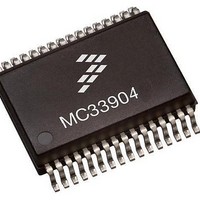
MCZ33904B3EK Freescale Semiconductor, MCZ33904B3EK Datasheet - Page 15

MCZ33904B3EK
Manufacturer Part Number
MCZ33904B3EK
Description
IC SBC CAN HS 3.3V 32SOIC
Manufacturer
Freescale Semiconductor
Type
High Speed CAN Interfacer
Specifications of MCZ33904B3EK
Operating Supply Voltage
3.3 V
Supply Current
2 mA
Package / Case
SOIC-32
Mounting Style
SMD/SMT
Product
CAN
Lead Free Status / RoHS Status
Lead free / RoHS Compliant
Available stocks
Company
Part Number
Manufacturer
Quantity
Price
Company:
Part Number:
MCZ33904B3EKR2
Manufacturer:
FREESCA
Quantity:
4 975
Table 4. 33903/4/5 Pin Definitions (continued)
Analog Integrated Circuit Device Data
Freescale Semiconductor
33905D
54 Pin
A functional description of each pin can be found in the
26
36
37
38
39
40
41
42
43
44
45
46
33905S
32 Pin
N/A
17
18
19
20
21
22
23
24
25
26
27
32 Pin
33904
N/A
N/A
N/A
N/A
20
21
22
23
24
25
26
27
32 Pin
33903
N/A
N/A
N/A
N/A
N/A
N/A
22
23
24
25
26
27
33903D
32 Pin
N/A
17
19
20
21
22
23
24
25
26
27
28
33903S
32 Pin
N/A
N/A
19
20
21
22
23
24
25
26
27
28
33903P
32 Pin
N/A
N/A
N/A
N/A
N/A
22
23
24
25
26
27
28
Functional Pin Description
Pin Name
33903D/5D
33903S/5S
33903D/5D
33903S/5S
33903D/5D
33903S/5S
VSENSE
TXD-L11
RXD-L1
RXD-L
SCLK
MOSI
MISO
TXD-L
I/O-1
LIN2
LIN-1
RST
INT
LIN
CS
Function
Output
Output
Output
Output
Output
Output
Output
Input/
Input/
Input/
Input
Input
Input
Input
Input
Pin
(Active LOW)
(Active LOW)
(Active LOW)
Reset Output
LIN Transmit
Input Output
LIN Receive
Sense input
Master Out /
Chip Select
Serial Data
Master In /
Slave Out
Interrupt
Slave In
Formal
LIN bus
LIN bus
Output
Name
Clock
Data
Data
1
section beginning on
LIN bus input output connected to the
LIN bus.
LIN bus input output connected to the
LIN bus.
LIN bus transmit data input. Includes
an internal pull-up resistor to VDD.
LIN bus receive data output.
Direct battery voltage input sense. A
serial resistor is required to limit the
input current during high voltage
transients.
Configurable pin as an input or
output, for connection to external
circuitry (switched or small load). The
voltage level can be read by the SPI
and the MUX output pin. The input
can be used as a programmable
Wake-up input in (LP) mode. It can
be used in association with
I/O-0 for a cyclic sense function in
(LP) mode.
This is the device reset output whose
main function is to reset the MCU.
This pin has an internal pull-up to
VDD
monitored in order to detect external
reset and safe conditions.
This output is asserted low when an
enabled interrupt condition occurs.
This pin is an open drain structure
with an internal pull up resistor to
VDD.
Chip select pin for the SPI. When the
CS is low, the device is selected. In
(LP) mode with V
on CS is a Wake-up condition
Clock input for the Serial Peripheral
Interface (SPI) of the device
SPI data received by the device
SPI data sent to the MCU. When the
CS is high, MISO is high-impedance
.
The reset input voltage is also
Definition
page
DD
PIN DEFINITIONS
ON, a transition
35.
33903/4/5
15


