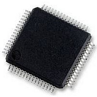
HD64F36077GHV Renesas Electronics America, HD64F36077GHV Datasheet - Page 64

HD64F36077GHV
Manufacturer Part Number
HD64F36077GHV
Description
16BIT MCU FLASH 56K, SMD, LQFP64
Manufacturer
Renesas Electronics America
Datasheet
1.HD64F36077GHV.pdf
(524 pages)
Specifications of HD64F36077GHV
No. Of I/o's
47
Ram Memory Size
4KB
Cpu Speed
20MHz
No. Of Timers
4
Digital Ic Case Style
LQFP
Supply Voltage Range
4.5V
Core Size
16bit
Program Memory Size
56KB
Oscillator Type
External Only
Controller Family/series
H8/300H
Peripherals
ADC
Rohs Compliant
Yes
Lead Free Status / RoHS Status
Lead free / RoHS Compliant
Available stocks
Company
Part Number
Manufacturer
Quantity
Price
Company:
Part Number:
HD64F36077GHV
Manufacturer:
RENESAS
Quantity:
340
Part Number:
HD64F36077GHV
Manufacturer:
RENESAS/瑞萨
Quantity:
20 000
- Current page: 64 of 524
- Download datasheet (4Mb)
Section 2 CPU
2.6
CPU operation is synchronized by a system clock (φ) or a subclock (φ
edge of φ or φ
three states. The cycle differs depending on whether access is to on-chip memory or to on-chip
peripheral modules.
2.6.1
Access to on-chip memory takes place in two states. The data bus width is 16 bits, allowing access
in byte or word size. Figure 2.9 shows the on-chip memory access cycle.
Rev. 1.00 Sep. 16, 2005 Page 34 of 490
REJ09B0216-0100
Basic Bus Cycle
Access to On-Chip Memory (RAM, ROM)
SUB
to the next rising edge is called one state. A bus cycle consists of two states or
ø or ø
Internal address bus
Internal read signal
Internal data bus
(read access)
Internal write signal
Internal data bus
(write access)
SUB
Figure 2.9 On-Chip Memory Access Cycle
T
1
state
Bus cycle
Address
Write data
Read data
T
2
state
SUB
). The period from a rising
Related parts for HD64F36077GHV
Image
Part Number
Description
Manufacturer
Datasheet
Request
R

Part Number:
Description:
KIT STARTER FOR M16C/29
Manufacturer:
Renesas Electronics America
Datasheet:

Part Number:
Description:
KIT STARTER FOR R8C/2D
Manufacturer:
Renesas Electronics America
Datasheet:

Part Number:
Description:
R0K33062P STARTER KIT
Manufacturer:
Renesas Electronics America
Datasheet:

Part Number:
Description:
KIT STARTER FOR R8C/23 E8A
Manufacturer:
Renesas Electronics America
Datasheet:

Part Number:
Description:
KIT STARTER FOR R8C/25
Manufacturer:
Renesas Electronics America
Datasheet:

Part Number:
Description:
KIT STARTER H8S2456 SHARPE DSPLY
Manufacturer:
Renesas Electronics America
Datasheet:

Part Number:
Description:
KIT STARTER FOR R8C38C
Manufacturer:
Renesas Electronics America
Datasheet:

Part Number:
Description:
KIT STARTER FOR R8C35C
Manufacturer:
Renesas Electronics America
Datasheet:

Part Number:
Description:
KIT STARTER FOR R8CL3AC+LCD APPS
Manufacturer:
Renesas Electronics America
Datasheet:

Part Number:
Description:
KIT STARTER FOR RX610
Manufacturer:
Renesas Electronics America
Datasheet:

Part Number:
Description:
KIT STARTER FOR R32C/118
Manufacturer:
Renesas Electronics America
Datasheet:

Part Number:
Description:
KIT DEV RSK-R8C/26-29
Manufacturer:
Renesas Electronics America
Datasheet:

Part Number:
Description:
KIT STARTER FOR SH7124
Manufacturer:
Renesas Electronics America
Datasheet:

Part Number:
Description:
KIT STARTER FOR H8SX/1622
Manufacturer:
Renesas Electronics America
Datasheet:


