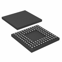
ADUC7121BBCZ-RL Analog Devices Inc, ADUC7121BBCZ-RL Datasheet - Page 18

ADUC7121BBCZ-RL
Manufacturer Part Number
ADUC7121BBCZ-RL
Description
PRECISION ANALOG MCU I.C
Manufacturer
Analog Devices Inc
Series
MicroConverter® ADuC7xxxr
Datasheet
1.ADUC7121BBCZ.pdf
(96 pages)
Specifications of ADUC7121BBCZ-RL
Core Processor
ARM7
Core Size
16/32-Bit
Speed
41.78MHz
Connectivity
I²C, SPI, UART/USART
Peripherals
POR, PWM, WDT
Number Of I /o
32
Program Memory Size
126KB (63K x 16)
Program Memory Type
FLASH
Ram Size
8K x 8
Voltage - Supply (vcc/vdd)
3 V ~ 3.6 V
Data Converters
A/D 9x12b, D/A 4x12b
Oscillator Type
Internal
Operating Temperature
-10°C ~ 95°C
Package / Case
108-LFBGA, CSPBGA
Lead Free Status / RoHS Status
Lead free / RoHS Compliant
Eeprom Size
-
Lead Free Status / RoHS Status
Lead free / RoHS Compliant
Other names
ADUC7121BBCZ-RL
ADUC7121BBCZ-RLTR
ADUC7121BBCZ-RLTR
Available stocks
Company
Part Number
Manufacturer
Quantity
Price
Company:
Part Number:
ADUC7121BBCZ-RL
Manufacturer:
Analog Devices Inc
Quantity:
10 000
ADuC7121
Pin No.
D1
E1
E2
F2
D12
E12
L8
L5
B8
K6
K7
L6
M5
L7
M8
K5
K4
M4
L4
K3
M3
M10
M9
L9
K9
K8
K1
K2
J2
L2
M2
L3
M11
L11
L10
K10
K11
K12
B5
C6
Mnemonic
P3.2/IRQ4/PWM3/PLAO[2]
P3.3/IRQ5/PWM4/PLAO[3]
P3.4/PLAO[8]
P3.5/PLAO[9]
P3.6/PLAO[10]
P3.7/BM/PLAO[11]
V
V
I
BUF_VREF1
BUF_VREF2
PADC0P
PADC0N
PADC1P
PADC1N
NC
NC
NC
NC
ADC4
ADC5
ADC6
ADC7
ADC8
ADC9
ADC10/AINCM
DAC0
DAC1
NC
NC
NC
NC
DAC2
NC
NC
NC
NC
DAC3
IDAC4
PVDD_IDAC4
REF
REF
REF
_2.5
_1.2
Type
I/O
I/O
I/O
I/O
I/O
I/O
AI/O
AI/O
AI/O
AO
AO
AI
AI
AI
AI
NC
NC
NC
NC
AI
AI
AI
AI
AI
AI
AI
NC
NC
NC
NC
AO
NC
NC
NC
NC
AO
AO
S
AO
AO
1
Description
General-Purpose Input and Output Port 3.2 (P3.2).
External Interrupt Request 4, Active High (IRQ4).
Pulse-Width Modulator 3 Output (PWM3).
Programmable Logic Array for Output Element 2 (PLAO[2]).
General-Purpose Input and Output Port 3.3 (P3.3).
External Interrupt Request 5, Active High (IRQ5).
Pulse-Width Modulator 4 Output (PWM4).
Programmable Logic Array for Output Element 3 (PLAO[3]).
General-Purpose Input and Output Port 3.4 (P3.4).
Programmable Logic Array for Output Element 8 (PLAO[8]).
General-Purpose Input and Output Port 3.5 (P3.5).
Programmable Logic Array for Output Element 9 (PLAO[9]).
General-Purpose Input and Output Port 3.6 (P3.6).
Programmable Logic Array for Output Element 10 (PLAO[10]).
Programmable Logic Array for Output Element 11 (PLAO[11]).
2.5 V Reference Output and External 2.5 V Reference Input.
1.2 V Reference Output and External 1.2 V Reference Input. Cannot be used to source
current externally.
Generates Reference Current for IDACs. Set by the external resistor, R
Buffered 2.5 V. The maximum load for BUF_VREF1 is 1.2 mA.
Buffered 2.5 V. The maximum load for BUF_VREF2 is 1.2 mA.
PGA Channel 0+.
PGA Channel 0−.
PGA Channel 1+.
PGA Channel 1−.
No Connect. Do not connect to this pin.
No Connect. Do not connect to this pin.
No Connect. Do not connect to this pin.
No Connect. Do not connect to this pin.
Single-Ended or Differential Analog Input 4.
Single-Ended or Differential Analog Input 5.
Single-Ended or Differential Analog Input 6.
Single-Ended or Differential Analog Input 7.
Single-Ended or Differential Analog Input 8.
Single-Ended or Differential Analog Input 9.
Single-Ended or Differential Analog Input 10 (ADC10).
Common Mode (AINCM). The common-mode function of this pin is for pseudo
differential input.
No Connect. Do not connect to this pin.
No Connect. Do not connect to this pin.
No Connect. Do not connect to this pin.
No Connect. Do not connect to this pin.
12-Bit DAC2 Output.
No Connect. Do not connect to this pin.
No Connect. Do not connect to this pin.
No Connect. Do not connect to this pin.
No Connect. Do not connect to this pin.
12-Bit DAC3 Output.
IDAC4 Output. The maximum output for this pin is 20 mA.
2.0 V Power for IDAC4.
General-Purpose Input and Output Port 3.7 (P3.7).
12-Bit DAC0 Output.
12-Bit DAC1 Output.
Rev. 0 | Page 18 of 96
EXT
.


