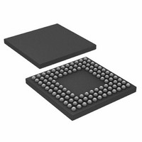
ADUC7121BBCZ-RL Analog Devices Inc, ADUC7121BBCZ-RL Datasheet - Page 9

ADUC7121BBCZ-RL
Manufacturer Part Number
ADUC7121BBCZ-RL
Description
PRECISION ANALOG MCU I.C
Manufacturer
Analog Devices Inc
Series
MicroConverter® ADuC7xxxr
Datasheet
1.ADUC7121BBCZ.pdf
(96 pages)
Specifications of ADUC7121BBCZ-RL
Core Processor
ARM7
Core Size
16/32-Bit
Speed
41.78MHz
Connectivity
I²C, SPI, UART/USART
Peripherals
POR, PWM, WDT
Number Of I /o
32
Program Memory Size
126KB (63K x 16)
Program Memory Type
FLASH
Ram Size
8K x 8
Voltage - Supply (vcc/vdd)
3 V ~ 3.6 V
Data Converters
A/D 9x12b, D/A 4x12b
Oscillator Type
Internal
Operating Temperature
-10°C ~ 95°C
Package / Case
108-LFBGA, CSPBGA
Lead Free Status / RoHS Status
Lead free / RoHS Compliant
Eeprom Size
-
Lead Free Status / RoHS Status
Lead free / RoHS Compliant
Other names
ADUC7121BBCZ-RL
ADUC7121BBCZ-RLTR
ADUC7121BBCZ-RLTR
Available stocks
Company
Part Number
Manufacturer
Quantity
Price
Company:
Part Number:
ADUC7121BBCZ-RL
Manufacturer:
Analog Devices Inc
Quantity:
10 000
Parameter
ESD TESTS
1
2
3
4
5
6
7
8
9
10
11
12
13
14
15
16
All ADC channel specifications are guaranteed during normal MicroConverter core operation.
Apply to all ADC input channels.
Measured using the factory set default values in the ADC offset register (ADCOF) and gain coefficient register (ADCGN).
Not production tested but supported by design and/or characterization data on production release.
Measured using the factory set default values in ADCOF and ADCGN with an external
system components, the user may need to execute a system calibration to remove external endpoint errors and achieve these specifications (see the ADC section).
The input signal can be centered on any dc common-mode voltage (V
V
all VDACs are on. V
The PVDD_IDAC0 pad voltage must be at least 300 mV greater than the IDAC0 pad voltage. These voltages are measured via the PVDD0 and IDAC0 channels of the
ADC. This allows the IDAC0 pin to be pulled up to 1.7 V provided that this 300 mV differential voltage is maintained between the pads. This may require the
PVDD_IDAC0 being supplied with a voltage greater than 2.0 V. The 2.1 V maximum PVDD_IDACx rating must not be exceeded.
DAC linearity is calculated using a reduced code range of 100 to 3995.
DAC gain error is calculated using a reduced code range of 100 to internal 2.5 V V
Die temperature.
Endurance is qualified as per JEDEC Standard 22 Method A117 and measured at −40°C, +25°C, +85°C, and +125°C.
Retention lifetime equivalent at junction temperature (T
Test carried out with a maximum of eight I/Os set to a low output level.
using a 3.6 V supply, and sleep mode using 3.6 V supply.
IOV
Power supply current consumption is measured in normal, pause, and sleep modes under the following conditions: normal mode using a 3.6 V supply, pause mode
REF
Digital Power Supply Current
Additional Power Supply Currents
HBM Passed Up to
FICDM Passed Up to
calibration and trimming are performed under the following conditions: the core is operating in normal mode CD = 0, the ADC is on, the current DACs are on, and
DD
IOV
IOV
IOV
ADC
IDAC
DAC
power supply current increases typically by 2 mA during a Flash/EE erase cycle.
DD
DD
DD
Current in Normal Mode
Current in Pause Mode
Current in Sleep Mode
REF
accuracy may vary under other operating conditions.
4
4
Min
J
) = 85°C as per JEDEC Standard 22 Method A117. Retention lifetime derates with junction temperature.
Typ
7
11
30
25
100
2.7
21
250
CM
) provided that this value is within the ADC voltage input range specified.
Rev. 0 | Page 9 of 96
Max
40
4
0.5
REF
AD845
.
op amp as an input buffer stage as shown in Figure 23. Based on external ADC
Unit
mA
mA
mA
mA
μA
mA
mA
μA
kV
kV
Test Conditions/Comments
Code executing from Flash/EE
CD = 7
CD = 3
CD = 0 (41.78 MHz clock)
CD = 0 (41.78 MHz clock)
T
@1 MSPS
All current DACs (IDACs) on
per VDAC
2.5 V reference, T
A
= 25°C
A
= 25°C
ADuC7121


