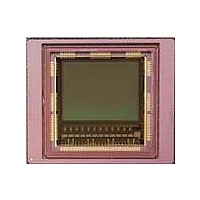
CYIL2SM1300AA-GZDC Cypress Semiconductor Corp, CYIL2SM1300AA-GZDC Datasheet
CYIL2SM1300AA-GZDC
Specifications of CYIL2SM1300AA-GZDC


Related parts for CYIL2SM1300AA-GZDC

CYIL2SM1300AA-GZDC Summary of contents
Page 1
... It packs 24 parallel 10-bit A/D converters with an aggregate conversion rate of 740 MSPS. On-chip digital column Ordering Information Marketing Part Number CYIL2SM1300AA-GZDC CYIL2SM1300AA-GZWC CYIL2SC1300AA-GZDC CYIL2SM1300-EVAL Note 1. Contact your local sales office for the windowless option. ...
Page 2
... Serial Peripheral Interface (SPI) ..................................17 Image Sensor Timing and Readout ................................18 Frame Rate and Windowing ........................................18 Operation and Signaling ..............................................19 Global Shutter .............................................................19 Pipelined Shutter .........................................................20 Document Number: 001-24599 Rev. *F CYIL2SM1300AA Triggered Shutter ........................................................22 Non Destructive Readout (NDR) .................................23 Image Format and Read Out Protocol ........................24 Additional Features ..........................................................29 Windowing ...................................................................29 Subsampling ................................................................29 Reverse Scan ...
Page 3
... Table 2. Electro Optical Specifications Parameter Conversion gain Full well charge Responsivity Fill factor Parasitic light sensitivity Dark noise FPN PRNU Dark signal Power dissipation Description CYIL2SM1300AA Value - 0.0325 DN DN/nJ/cm at 550 nm 40% <1/10000 1.2025 DN 35% at 550 nm 2% RMS of the output swing <1% RMS of the output signal ...
Page 4
... Clock enabled, lux=0 Clock enabled, lux=0 shutdown mode, lux=0 Clock enabled, lux=0 Clock enabled, lux=0 Shutdown mode, lux=0 Clock enabled, lux=0 Clock enabled, lux=0 Shutdown mode, lux=0 Clock enabled, lux=0 Clock enabled, lux=0 Shutdown mode, lux=0 CYIL2SM1300AA Min Typ Max Units -5% 2.5 + ...
Page 5
... Digital Group of +2.5V supply: V ■ Combine V PRECH Table 4. Condition Blocks in standby with SPI upload lux = 0, clock = 315 MHz, 500 fps [5] Condition fps = 500 At maximum clock At maximum clock peak-to-peak Maximum clock speed CYIL2SM1300AA Min Typ Max 1.8 2.5 3.675 0 1.8 2.2 3.675 0 -5% 2 ...
Page 6
... The LVDS interface can receive high speed Photovoltaic Response Curve Figure 2. Photovoltaic Response of LUPA 1300-2 Document Number: 001-24599 Rev. *F CYIL2SM1300AA and wide bandwidth data signals and maintain low noise and distortion. A special training mode enables the receiving system to synchronize the incoming data stream when switching to master, slave, or triggered mode ...
Page 7
... Spectral Response Curve Figure 3. Spectral Response of LUPA 1300-2 Mono and Color 0.35 0.3 0.25 0.2 0.15 0.1 0.05 0 400 500 Document Number: 001-24599 Rev. *F 600 700 800 Wavelength (nm) CYIL2SM1300AA 900 1000 Page [+] Feedback ...
Page 8
... Color Filter Array The color version of LUPA 1300-2 is available in Bayer (RGB) patterned color filter array. The orientation of RGB is shown in Document Number: 001-24599 Rev. *F Figure 4. RGB Bayer CYIL2SM1300AA Figure 4. Page [+] Feedback ...
Page 9
... Msps 31.5 MHz Local register Data block 63 MHz 63 Msps LVDS TX and RX 315 MHz 12x LVDS outputs at 630 Msps Figure 6. 6T Pixel Architecture Vpix on page 3. This Reset CYIL2SM1300AA SPI & Logic Clk in Clock Divider Clk out Vmem Sample Select Page [+] Feedback ...
Page 10
... It also contains a huge part of the functionality for black level calibration and FPN correction. A number of data blocks are placed in parallel to serve all data output channels. One additional channel generates the synchro- nization protocol. A high level overview is illustrated in the following figure. Figure 7. Data Block CYIL2SM1300AA Specification Page [+] Feedback ...
Page 11
... Pga settings [6] 0 Power down AFE [7:0] 0x00 Power down adc_channel_2x [3:0] 0x00 Power down adc_channel_2x CYIL2SM1300AA Se rializer Se rializer Se rializer clockgenerator clockgenerator LVD S LVD S LVD S LVD S Transmi tter Transmi tter Transmi tter Transmi tter ...
Page 12
... Overwrite incoming ADC data by the data in the testpat register [3] 0 Reserved, fixed value [5:4] 0x00 Pattern inserted to generate a test image [7:0] 0x00 Pattern inserted to generate a test image [0] 0 Bypass the data block [1] 0 Enables the FPN correction CYIL2SM1300AA Description Page [+] Feedback ...
Page 13
... Controls the granularity of the timer settings (only for those that have ‘granularity selectable’ in the description): ‘0’: Expressed in number of lines ‘1’: Expressed in clock cycles (multiplied by 2**seqmode4[3:0]) CYIL2SM1300AA Description Page [+] Feedback ...
Page 14
... Length of integration time (granularity selectable) [7:0] 0x40 Length of DS integration time (granularity selectable) [1:0] 0x00 Length of DS integration time (granularity selectable) [7:0] 0x0C Length of TS integration time (granularity selectable) [1:0] 0x00 Length of TS integration time (granularity selectable) CYIL2SM1300AA Description Page [+] Feedback ...
Page 15
... No CRC is calculated for that value. From then on, every incoming pixel is updated through the regular CRC. ■ Training and test pattern generation CYIL2SM1300AA Description Page [+] Feedback ...
Page 16
... X3_kernels (71, 6 bit). This register sets the number of kernels or X width to be read out for window 3 (if enabled). Y4_start (72 and 73, 10 bit). These registers set the Y start address for window 4 (if enabled). X4_start (73, 6bit). This register sets the X start address for window 4 (if enabled). CYIL2SM1300AA Page [+] Feedback ...
Page 17
... SPI uploads stored on the chip. The SPI clock speed must be slower by a factor of 30 when compared to the system clock (315 MHz nominal speed). Figure 9. Write Access (C='1') Figure 10. Read Access (C='0') CYIL2SM1300AA Figure 9 and Page [+] Feedback ...
Page 18
... MHz data rate Figure 11. Timing Diagram Table 11. Typical Frame Rates at 315 MHz Image Resolution (X*Y) 1296x1024 1008x1000 816x600 648x480 528x512 264x256 144x128 24x2 CYIL2SM1300AA Frame Read Frame Rate (fps) Out Time (ms) 1.9760 506 1.5807 633 0.7997 1250 0.5370 1862 0.4887 2046 0 ...
Page 19
... System clock (315 MHz) SPI chip select Clock of the SPI (< Sensor clock/30) Data line of the SPI, serial input Data line of the SPI, serial output Triggered Shutter on page 22) mode. Figure 12. Global Shutter Operation Burst Readout ti CYIL2SM1300AA Figure 12 shows the Time axis Page [+] Feedback ...
Page 20
... This mode is called master mode. The second option is to drive the integration time through an external pin. This mode is called slave mode. CYIL2SM1300AA Expo sure N Page ...
Page 21
... Ensure that the added value of the registers res_length and tint_timer always exceeds the number of lines that are read out. This is because the sequencer samples a new image after integration is complete, without checking if image readout is finished. Enlarging res_length to accommodate for this has no impact on image capture. Document Number: 001-24599 Rev. *F CYIL2SM1300AA Page [+] Feedback ...
Page 22
... Synchronize external flash with exposure ■ Apply extremely long integration times (only in slave mode) Document Number: 001-24599 Rev. *F Figure 15. When the input pin int_time is asserted, the pixel Exposure Time FOT Reset FOT FOT FOT Readout N CYIL2SM1300AA Reset Readout N+1 N+1 Page [+] Feedback ...
Page 23
... When nr_of_ndr_steps is two, there is one reset and two register. If samples, and so on. In the slave mode, nothing changes on the protocol of the signals int_time_*. The sequencer suppresses the internal reset signal to the pixel array. CYIL2SM1300AA time Table 14 on page 23 summarizes the Page [+] Feedback ...
Page 24
... Pixels are always read in multiples of 24 (one value to every channel in the AFE). The last time slot contains not only valid pixels, but also two dummy columns, six grey columns, and eight black columns. Document Number: 001-24599 Rev. *F Figure 18. Before the actual pixels are read out, one dummy Figure 18. Sensor Read Out Format CYIL2SM1300AA Page [+] Feedback ...
Page 25
... CYIL2SM1300AA Figure 7. The synchroni- Table 15. Note that a FS also serves ch7 ch8 ch9 ch10 ch11 ...
Page 26
... CYIL2SM1300AA ch8 ch9 ch10 ch11 1265 1267 1269 1271 1279 1277 1275 1273 1278 1276 1274 1272 ch8 ch9 ch10 ch11 1279 1277 1275 1273 ...
Page 27
... Sequencer internal state Data Channel Sync Channel Data Channel Sync Channel Document Number: 001-24599 Rev. *F Line FOT ROT black ROT ROT line Ys Ys timeslot timeslot timeslot X X+1 53 CYIL2SM1300AA Figure 19. A clear distinction is made with line Ye ROT timeslot CRC 54 timeslot Page [+] Feedback ...
Page 28
... Although the window is defined as not containing black line Ys line FOT ROT ROT ROT Ys timeslot timeslot timeslot timeslot Xstart Xend-1 Xend 54. The dummy black line again spans the entire width of CYIL2SM1300AA line Ye ROT timeslot CRC 54 timeslot Single Window Mode Containing Page [+] Feedback ...
Page 29
... Subsampling Subsampling reduces resolution while maintaining the constant field of view and an increased frame rate. LUPA1300-2 supports monochrome and color subsampling modes of operation. The pixel order for one complete row is shown page 26. CYIL2SM1300AA 1024 pixels Table 18 and Table Page [+] Feedback ...
Page 30
... Document Number: 001-24599 Rev result, the line numbers always increment. When reverse scanning in X, the Figure 24. Normal and Reverse Scanning in Y Figure 26. Readout from Windows FS Window 2 FE FOT FS CYIL2SM1300AA Figure 26. Also, the sum of readout times of all Figure 25 shows how to configure Window 1 FE ROT FS ...
Page 31
... Figure 28 By choosing the time stamps of the double and triple slope resets (typical at 90% and 99% of the integration, configurable by the user possible to have a nonsaturated pixel value even for pixels that receive a huge amount of light. CYIL2SM1300AA Readout N Window 2 t Page [+] Feedback ...
Page 32
... You must configure the multiple slope parameters for the application and interpret the pixel data accordingly. Document Number: 001-24599 Rev. *F Figure 29. Triple Slope Timing in Master Mode Figure 30. Triple Slope Timing in Slave Mode CYIL2SM1300AA Page [+] Feedback ...
Page 33
... The registers used to configure the correction are: Figure 31. Dark Image Without FPN Correction (5x Amplified) Figure 32. Dark Image With FPN Correction Enabled (5x Amplified) Document Number: 001-24599 Rev. *F CYIL2SM1300AA ■ datachannelX_1 with X from 0 to 11. The field [1] of these registers enables the offset corrections of the specific output channel ...
Page 34
... Calculate the average value of this grey (or black) data; also average it out over the different grey columns. 5. Adapt the DACVREFADC if the calculated value deviate from the desired black level value and return to step (2). 6. Repeat the procedure for temperature changes. CYIL2SM1300AA Figure 33 shows the internal state of the line ROT ...
Page 35
... C 133 132 129 126 123 120 117 114 111 108 105 102 135 139 140 137 145 * 5 U 136 144 141 138 146 * 8 V 149 147 142 * 150 148 143 * Document Number: 001-24599 Rev TOP VIEW CYIL2SM1300AA Page [+] Feedback ...
Page 36
... ADC ground I/O ADC power I/O LVDS power O p output channel [ output channel [ output channel [10 output channel [10 output channel [11 output channel [11] not assigned not assigned I/O LVDS ground I/O ADC ground CYIL2SM1300AA Position V10 W10 T10 U11 T11 U10 V11 W11 ...
Page 37
... DFT scan enable; Customer: connect to ground I DFT clock; Customer: connect to ground I DFT clock enable; Customer: connect to ground I/O pixel core ground I/O digital ground I/O digital power supply I/O pixel core supply CYIL2SM1300AA Position T17 U18 V19 W19 V20 W20 W24 V24 W22 V22 U20 ...
Page 38
... I/O digital power supply I/O digital ground I/O pixel core ground not assigned not assigned not assigned not assigned O ADC common mode decoupling I/O pixel core supply CYIL2SM1300AA Position A18 C17 B17 A17 C16 B16 A16 C15 B15 A15 C14 B14 ...
Page 39
... I/O column buffers supply I/O column buffers ground I/O digital ground I/O ADC power supply I/O ADC ground I/O higher limit ADC range decoupling I/O lower limit ADC range decoupling I/O digital power supply I/O digital ground CYIL2SM1300AA Position ...
Page 40
... Pb-free wave soldering profile for pin grid array package if no socket is used Recommended Andon Electronics (www.andonelectronics.com) Socket Manufacturer Document Number: 001-24599 Rev. *F Description Min - 400 Figure 36 BGA Socket: 10-24-05-168-319T-P27-L14 Thru Hole: 10-24-05-168-347T-P27-L14 CYIL2SM1300AA Typ Max Units 750 NA µm -42 NA µm -150 NA µ deg 0 1 deg 0 50 µ deg -121 NA µm ...
Page 41
... Package Drawing Figure 35. Package Outline Drawing for the LUPA 1300-2 168-Pin µPGA Document Number: 001-24599 Rev. *F CYIL2SM1300AA 001-44705 *A Page [+] Feedback ...
Page 42
... Products returned to Cypress for failure analysis should be handled under these same conditions and packed in its original packing materials, or the customer may be liable for the product. Document Number: 001-24599 Rev. *F CYIL2SM1300AA Figure 36 shows the transmission Application Note References ■ AN54468: Interfacing the LUPA1300-2 with FPGA. ...
Page 43
... Document History Page Document Title: CYIL2SM1300AA LUPA 1300-2: High Speed CMOS Image Sensor Document Number: 001-24599 Revision ECN Orig. of Change ** 1438663 FPW *A 2649816 NVEA/AESA *B 2745961 NVEA/AESA *C 2765859 NVEA/AESA *D 2800053 NVEA/UUA *E 2868919 NVEA *F 2883368 NVEA Sales, Solutions, and Legal Information Worldwide Sales and Design Support Cypress offers standard and customized CMOS image sensors for consumer as well as industrial and professional applications ...