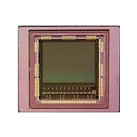
CYIL2SM1300AA-GZDC Cypress Semiconductor Corp, CYIL2SM1300AA-GZDC Datasheet - Page 20

CYIL2SM1300AA-GZDC
Manufacturer Part Number
CYIL2SM1300AA-GZDC
Description
IMAGE SENSOR CMOS LUPA-1300-3
Manufacturer
Cypress Semiconductor Corp
Type
CMOS Imagingr
Specifications of CYIL2SM1300AA-GZDC
Package / Case
168-PGA
Pixel Size
14µm x 14µm
Active Pixel Array
1280H x 1024V
Frames Per Second
500
Voltage - Supply
2.5V, 3.3V
Operating Supply Voltage
2.5 V
Maximum Power Dissipation
1350 mW
Maximum Operating Temperature
+ 70 C
Supply Current
80 mA
Minimum Operating Temperature
0 C
Package
168CuPGA
Image Size
1280x1024 Pixels
Color Sensing
Monochrome
Operating Temperature
0 to 70 °C
Lead Free Status / RoHS Status
Lead free / RoHS Compliant
Lead Free Status / RoHS Status
Lead free / RoHS Compliant, Lead free / RoHS Compliant
The timing of the sensor consists of two parts. The first part is
related to the exposure time and the control of the pixel. The
second part is related to the read out of the image sensor.
Integration and readout are in parallel or triggered. In the first
case, the integration time of frame I is ongoing during the readout
of frame I-1.
The readout of every frame starts with a FOT, during which the
analog value on the pixel diode is transferred to the pixel memory
element. After this FOT, the sensor is read out line by line. The
read out of every line starts with a ROT, during which the pixel
value is put on the column lines. Then the pixels are selected in
Pipelined Shutter
Integration and readout occur in parallel and are continuous. You
only need to start and stop the batch of image captures.
Integration of frame N is always ongoing during readout of frame
N-1. The readout of every frame starts with a FOT, during which
the analog value on the pixel diode is transferred to the pixel
memory element. After this FOT, the sensor is read out line by
line. The readout of every line starts with a ROT, during which the
pixel value is put on the column lines. Then the pixels are muxed
Document Number: 001-24599 Rev. *F
In teg ra tion T im e
Ha n dling
Re a do ut
Ha n dling
Figure 13
shows this parallel timing structure.
R O T
F O T
L ine R ea dou t
Reset
N
Rea do u t F ra m e N- 1
Figure 13. Global Readout Timing (Parallel)
Expo sur e T im e N
groups of 24 (12 on rising edge, and 12 on the falling edge of the
internal clock). So in total, 54 kernels of 24 pixels are read out
every line. The internal timing is generated by the sequencer.
The sequencer can operate in two modes: master mode and
slave mode. In master mode, all internal timing is controlled by
the sequencer, based on the SPI settings. In slave mode, the
integration timing is directly controlled by over three pins, and the
readout timing is still controlled by the sequencer. The
seqmode1[1] register of the SPI selects between the master and
slave modes.
in the correct ADCs, processed, and then sent to the LVDS
output block.
You have two options in the pipelined shutter mode. The first
option is to program the reset and integration through the config-
uration interface and let the sequencer handle integration time
automatically. This mode is called master mode. The second
option is to drive the integration time through an external pin.
This mode is called slave mode.
FO T
FO T
Re se t
N+1
Rea do ut F ra m e N
Expo sure T im e N+1
CYIL2SM1300AA
F O T
F O T
Page 20 of 43
[+] Feedback


