CYIL2SM1300AA-GZDC Cypress Semiconductor Corp, CYIL2SM1300AA-GZDC Datasheet - Page 19
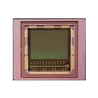
CYIL2SM1300AA-GZDC
Manufacturer Part Number
CYIL2SM1300AA-GZDC
Description
IMAGE SENSOR CMOS LUPA-1300-3
Manufacturer
Cypress Semiconductor Corp
Type
CMOS Imagingr
Specifications of CYIL2SM1300AA-GZDC
Package / Case
168-PGA
Pixel Size
14µm x 14µm
Active Pixel Array
1280H x 1024V
Frames Per Second
500
Voltage - Supply
2.5V, 3.3V
Operating Supply Voltage
2.5 V
Maximum Power Dissipation
1350 mW
Maximum Operating Temperature
+ 70 C
Supply Current
80 mA
Minimum Operating Temperature
0 C
Package
168CuPGA
Image Size
1280x1024 Pixels
Color Sensing
Monochrome
Operating Temperature
0 to 70 °C
Lead Free Status / RoHS Status
Lead free / RoHS Compliant
Lead Free Status / RoHS Status
Lead free / RoHS Compliant, Lead free / RoHS Compliant


Operation and Signaling
Digital Signals
Depending on the operation mode (Master or Slave), the pixel array of the image sensor requires different digital control signals. The
function of each signal is listed in this table.
Table 12. Overview of Digital Signals
Global Shutter
In a global shutter, light integration occurs on all pixels in parallel, although subsequent readout is sequential.
integration and readout sequence for the global shutter. All pixels are light sensitive at the same period of time. The whole pixel core
is reset simultaneously, and after the integration time, all pixel values are sampled together on the storage node inside each pixel.
The pixel core is read out line by line after integration. Note that the integration and readout cycle can occur in parallel (refer to
Pipelined Shutter
Document Number: 001-24599 Rev. *F
MONITOR_1
MONITOR_2
MONITOR_3
INT_TIME_3
INT_TIME_2
INT_TIME_1
RESET_N
CLK
SPI_CS
SPI_CLK
SPI_IN
SPI_OUT
Signal Name
on page 20) or in sequential (refer to
Output
Output
Output
Input
Input
Input
Input
Input
Input
Input
Input
Output
Line number
I/O
Integration Time
Output pin for integration timing, high during integration
Output pin for dual slope integration timing, high during integration
Output pin for triple slope integration timing, high during integration
Integration pin triple slope
Integration pin dual slope
Integration pin first slope
Sequencer reset, active LOW
System clock (315 MHz)
SPI chip select
Clock of the SPI (< Sensor clock/30)
Data line of the SPI, serial input
Data line of the SPI, serial output
Figure 12. Global Shutter Operation
Triggered Shutter
on page 22) mode.
Comments
Burst Readout
ti
Time axis
CYIL2SM1300AA
Figure 12
Page 19 of 43
shows the
[+] Feedback
Related parts for CYIL2SM1300AA-GZDC
Image
Part Number
Description
Manufacturer
Datasheet
Request
R

Part Number:
Description:
BOARD EVAL IMG SENS LUPA-1300-2
Manufacturer:
Cypress Semiconductor Corp
Datasheet:
Part Number:
Description:
Manufacturer:
Cypress Semiconductor Corp
Datasheet:
Part Number:
Description:
Manufacturer:
Cypress Semiconductor Corp
Datasheet:
Part Number:
Description:
Manufacturer:
Cypress Semiconductor Corp
Datasheet:
Part Number:
Description:
Manufacturer:
Cypress Semiconductor Corp
Datasheet:
Part Number:
Description:
Manufacturer:
Cypress Semiconductor Corp
Datasheet: