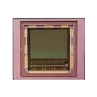
CYIL2SM1300AA-GZDC Cypress Semiconductor Corp, CYIL2SM1300AA-GZDC Datasheet - Page 11

CYIL2SM1300AA-GZDC
Manufacturer Part Number
CYIL2SM1300AA-GZDC
Description
IMAGE SENSOR CMOS LUPA-1300-3
Manufacturer
Cypress Semiconductor Corp
Type
CMOS Imagingr
Specifications of CYIL2SM1300AA-GZDC
Package / Case
168-PGA
Pixel Size
14µm x 14µm
Active Pixel Array
1280H x 1024V
Frames Per Second
500
Voltage - Supply
2.5V, 3.3V
Operating Supply Voltage
2.5 V
Maximum Power Dissipation
1350 mW
Maximum Operating Temperature
+ 70 C
Supply Current
80 mA
Minimum Operating Temperature
0 C
Package
168CuPGA
Image Size
1280x1024 Pixels
Color Sensing
Monochrome
Operating Temperature
0 to 70 °C
Lead Free Status / RoHS Status
Lead free / RoHS Compliant
Lead Free Status / RoHS Status
Lead free / RoHS Compliant, Lead free / RoHS Compliant
LVDS Block
The LVDS block is positioned below the data block. It receives a differential clock signal, transmits differential data over the 12 data
channels, and transmits a LVDS clock signal and a synchronization signal over the clock and synchronization channel.
A number of LVDS transmitter blocks are placed in parallel to serve all data, clock, and synchronization output channels. A high level
overview is illustrated in the following figure.
The function of this block is to take 10 bits of the protocol block, serialize these bits, and converts them to an LVDS standard (TIA/EIA
644A) compatible differential output signal. The block must also provide a clock to the host, to allow data recovery. This clock is an
on-chip version of the clock coming from the host.
Sequencer and Logic
The sequencer generates the complete internal timing of the pixel array and the readout. The timing can be controlled by the user
through the SPI register settings. The sequencer operates on the same clock as the data block. This is a division by 10 of the input
clock (internally divided).
Table 9
Table 9. Internal Registers
Document Number: 001-24599 Rev. *F
MBS
(reserved)
LVDS clk
divider
AFE
Block
lists the internal registers. These registers are discussed in detail in
Fix1
Fix2
Fix3
Fix4
Fix5
lvdsmain
lvdspwd1
lvdspwd2
Fix6
afebias
afemode
afepwd1
afepwd2
Register Name Address [6..0]
Transmi tter
Transmi tter
Transmi tter
Transmi tter
Seria lizer
Seria lizer
Seria lizer
LVD S
LVD S
LVD S
LVD S
c lock
c lock
c lock
c lock
Serializer<0>
Serializer<0>
Transmitter
Transmitter
Transmitter
10
11
12
0
1
2
3
4
5
6
7
8
9
LVD S
LVD S
LVD S
<0 >
<0 >
<0 >
Figure 8. LVDS Block - High Level Overview
Field
[7:0]
[7:0]
[7:0]
[7:0]
[7:0]
[3:0]
[7:4]
[7:0]
[5:0]
[7:0]
[3:0]
[2:0]
[5:3]
[7:0]
[3:0]
[6]
[7]
[6]
Serializer <1>
Serializer <1>
Tra ns mitte r
Tra ns mitte r
Tra ns mitte r
LV DS
LV DS
LV DS
<1>
<1>
<1>
0x00
0xFF
0x00
0x00
‘0x08’
‘0110’
0
0x00
0
0
0
0x00
‘1000’
‘111’
‘000’
0
0x00
0x00
Reset Value
…
…
Serializer <11>
Serializer <11>
Trans mitter
Trans mitter
Trans mitter
LVD S
LVD S
LVD S
<1 1>
<1 1>
<1 1>
Reserved, fixed value
Reserved, fixed value
Reserved, fixed value
Reserved, fixed value
Reserved, fixed value
lvds trim
clkadc phase
Power down channel 7:0
Power down channel 13:8
Power down all channels
lvds test mode
Reserved, fixed value
afe current biasing
vrefp, vrefm settings
Pga settings
Power down AFE
Power down adc_channel_2x 7 to 0
Power down adc_channel_2x 11 to 8
Detailed Description of Internal Registers
clockgenerator
clockgenerator
Re ceive r
Re ceive r
Re ceive r
LVDS
LVDS
LVDS
Description
CYIL2SM1300AA
Transmi tter
Transmi tter
Transmi tter
Transmi tter
Se rializer
Se rializer
Se rializer
LVD S
LVD S
LVD S
LVD S
Synch
Synch
Synch
Synch
on page 15.
Page 11 of 43
[+] Feedback


