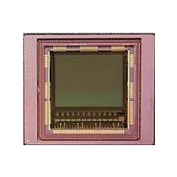
CYIL2SM1300AA-GZDC Cypress Semiconductor Corp, CYIL2SM1300AA-GZDC Datasheet - Page 15

CYIL2SM1300AA-GZDC
Manufacturer Part Number
CYIL2SM1300AA-GZDC
Description
IMAGE SENSOR CMOS LUPA-1300-3
Manufacturer
Cypress Semiconductor Corp
Type
CMOS Imagingr
Specifications of CYIL2SM1300AA-GZDC
Package / Case
168-PGA
Pixel Size
14µm x 14µm
Active Pixel Array
1280H x 1024V
Frames Per Second
500
Voltage - Supply
2.5V, 3.3V
Operating Supply Voltage
2.5 V
Maximum Power Dissipation
1350 mW
Maximum Operating Temperature
+ 70 C
Supply Current
80 mA
Minimum Operating Temperature
0 C
Package
168CuPGA
Image Size
1280x1024 Pixels
Color Sensing
Monochrome
Operating Temperature
0 to 70 °C
Lead Free Status / RoHS Status
Lead free / RoHS Compliant
Lead Free Status / RoHS Status
Lead free / RoHS Compliant, Lead free / RoHS Compliant
Table 9. Internal Registers (continued)
Detailed Description of Internal Registers
The registers must be changed only during idle mode, that is,
when seqmode1[0] is ‘0’. Uploaded registers have an immediate
effect on how the frame is read out. Parameters uploaded during
readout may have an undesired effect on the data coming out of
the images.
MBS Block
The register block contains registers for sensor testing and
debugging. All registers in this block must remain unchanged
after startup.
LVDS Clock Divider Block
This block controls division of the input clock for the LVDS
transmitters or receivers. This block also enables shutting down
one or all LVDS channels. For normal operation, this register
block must remain untouched after startup.
AFE Block
This register block contains registers to shut down ADC
channels or the complete AFE block. This block also contains the
register for setting the PGA gain: AFE_mode[5:3]. Refer to
Absolute Maximum Ratings
PGA settings.
Document Number: 001-24599 Rev. *F
Block
tint_black_timer 85
rot_timer
fot_timer
fot_timer
prechpix_timer
prechpix_timer
prechcol_timer
rowselect_timer 92
sample_timer
sample_timer
vmem_timer
vmem_timer
delayed_rdt_tim
er
delayed_rdt_tim
er
Fix29
Fix30
Fix31
Fix32
Fix33
Fix34
Register Name Address [6..0]
on page 3 for more details on the
86
87
88
89
90
91
93
94
95
96
97
98
99
100
101
102
103
104
Field
[7:0]
[7:0]
[7:0]
[1:0]
[7:0]
[7:0]
[7:0]
[1:0]
[7:0]
[1:0]
[7:0]
[7:0]
[7:0]
[1:0]
[0]
[0]
[0]
[0]
[0]
[0]
0x06
0x09
0x3B
0x01
0x7C
0x00
0x03
0x06
0xF8
0x00
0x10
0x01
0
0
0
0
0
0
0
0
Reset Value
Biasing Block
This block contains several registers for setting biasing currents
for the sensor. Default values after startup must remain
unchanged for normal operation of the sensor.
Image Core Block
The registers in this block have an impact on the pixel array itself.
Default settings after startup must remain unchanged for normal
operation of the image sensor.
Data Block
The data block is positioned in between the analog front end
(output stage + ADCs) and the LVDS interface. It muxes the
outputs of 2 ADCs to one LVDS block and performs some minor
data handling:
■
■
CRC calculation and insertion.
All data can be protected by a 10-bit checksum. The CRC10 is
calculated over all pixels between a Line Start and a Line End.
It is inserted in the data stream after the line is completed, if
input seq_data_crc is enabled.The polynomial used is
(x^10+x^9+x^6+x^3+x^2+x+1) and 10 bits are calculated in
parallel.When a new line is started, the seed is the first pixel
value of a line. No CRC is calculated for that value. From then
on, every incoming pixel is updated through the regular CRC.
Training and test pattern generation
Reserved, fixed value
Length of ROT (granularity clock cycles)
Length of FOT (granularity clock cycles)
Length of FOT (granularity clock cycles)
Length of pixel precharge (granularity clock cycles)
Length of pixel precharge (granularity clock cycles)
Length of column precharge (granularity clock cycles)
Length of rowselect (granularity clock cycles)
Length of pixel_sample (granularity clock cycles)
Length of pixel_sample (granularity clock cycles)
Length of pixel_vmem (granularity clock cycles)
Length of pixel_vmem (granularity clock cycles)
Readout delay for testing purposes (granularity selectable)
Readout delay for testing purposes (granularity selectable
Reserved, fixed value
Reserved, fixed value
Reserved, fixed value
Reserved, fixed value
Reserved, fixed value
Reserved, fixed value
Description
CYIL2SM1300AA
Page 15 of 43
[+] Feedback


