CYIL2SM1300AA-GZDC Cypress Semiconductor Corp, CYIL2SM1300AA-GZDC Datasheet - Page 5
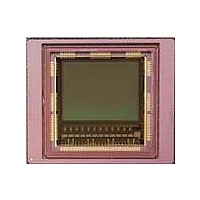
CYIL2SM1300AA-GZDC
Manufacturer Part Number
CYIL2SM1300AA-GZDC
Description
IMAGE SENSOR CMOS LUPA-1300-3
Manufacturer
Cypress Semiconductor Corp
Type
CMOS Imagingr
Specifications of CYIL2SM1300AA-GZDC
Package / Case
168-PGA
Pixel Size
14µm x 14µm
Active Pixel Array
1280H x 1024V
Frames Per Second
500
Voltage - Supply
2.5V, 3.3V
Operating Supply Voltage
2.5 V
Maximum Power Dissipation
1350 mW
Maximum Operating Temperature
+ 70 C
Supply Current
80 mA
Minimum Operating Temperature
0 C
Package
168CuPGA
Image Size
1280x1024 Pixels
Color Sensing
Monochrome
Operating Temperature
0 to 70 °C
Lead Free Status / RoHS Status
Lead free / RoHS Compliant
Lead Free Status / RoHS Status
Lead free / RoHS Compliant, Lead free / RoHS Compliant


Table 4. Power Supply Ratings
Boldface limits apply for T
Every module in the image sensor has its own power supply and
ground. The grounds can be combined externally, but not all
power supply inputs may be combined. Some power supplies
must be isolated to reduce electrical crosstalk and improve
shielding, dynamic range, and output swing. Internal to the
image sensor, the ground lines of each module are kept separate
to improve shielding and electrical crosstalk between them.
The LUPA 1300-2 contains circuitry to protect the inputs against
damage due to high static voltages or electric fields. However,
take normal precautions to avoid voltages higher than the
maximum rated voltages in this high impedance circuit. Unused
Table 5. Power Dissipation
Power supply specifications according to
Table 6. AC Electrical Characteristics
The following specifications apply for VDD = 2.5V, Clock = 315 MHz, 500 fps.
Note Duty Cycle Distortion and Jitter is passed directly from input to output. Therefore, DCD and Jitter tolerance depends on the
customer's system clock generation circuitry.
Document Number: 001-24599 Rev. *F
V
V
V
V
V
Power
Power
F
DC
DCD
fps
RES_DS
RES_TS
MEM_L
MEM_H
PRECH
CLK
CLK
Symbol
Symbol
Symbol
STDBY
[8]
Reset Dual
Slope Supply
Reset Triple
Slope Supply
Memory
Element low
level supply
Memory
Element high
level supply
Pre_charge
Driver Supply
Standby Power
Average Power Dissipation
Input Clock Frequency
Clock Duty Cycle
Duty Cycle Distortion
Jitter
Frame Rate
Power Supply
Parameter
Parameter
J
=T
[5]
MIN
[5, 6, 7]
Operating Voltage
Dynamic Current
Peak Current
Operating Voltage
Dynamic Current
Peak Current
Operating Voltage
Dynamic Current
Peak Current during FOT Clock enabled, lux=0
Peak Current during FOT Clock enabled, bright
Operating Voltage
Dynamic Current
Peak Current during FOT Clock enabled, lux=0
Operating Voltage
Dynamic Current
Peak Current during FOT Clock enabled, lux=0
Peak Current during FOT Clock enabled, lux=bright
to T
MAX
[5]
(continued)
Table
Parameter
, all other limits T
4.
Blocks in standby with SPI upload
lux = 0, clock = 315 MHz, 500 fps
fps = 500
At maximum clock
At maximum clock
peak-to-peak
Maximum clock speed
J
=+30°C. Clock = 315 MHz
Clock enabled, lux=0
Clock enabled, lux=0
Clock enabled, lux=0
Clock enabled, lux=0
Clock enabled, lux=0
Clock enabled, lux=0
Clock enabled, lux=0
inputs must always be tied to an appropriate logic level, for
example, V
ground through a 100 nF capacitor.
The recommended combinations of supplies are:
■
■
■
Analog group of +2.5V supply: V
V
Digital Group of +2.5V supply: V
Combine V
Condition
Condition
ADC
Condition
, V
pix
DD
, V
PRECH
or GND. All cap_xxx pins must be connected to
ANA
, V
and V
BUF
RES_AB
-10%
Min
-5%
-5%
1.8
1.8
to one supply
DIG
SAMPLE
CYIL2SM1300AA
, V
Typ
50
50
LVDS
Typ
2.5
0.4
2.2
0.3
2.5
0.2
3.3
0.7
0.3
36
14
62
30
45
32
25
1
, V
1350
Typ
400
RES_DS
Max
[8]
315
250
500
+10%
3.675
3.675
+5%
+5%
Max
3
2
1
3
Page 5 of 43
, V
MEM_L
Units
Units
MHz
Units
mW
mW
fps
ps
ps
%
mA
mA
mA
mA
mA
mA
mA
mA
mA
mA
mA
mA
V
V
V
V
V
,
[+] Feedback
Related parts for CYIL2SM1300AA-GZDC
Image
Part Number
Description
Manufacturer
Datasheet
Request
R

Part Number:
Description:
BOARD EVAL IMG SENS LUPA-1300-2
Manufacturer:
Cypress Semiconductor Corp
Datasheet:
Part Number:
Description:
Manufacturer:
Cypress Semiconductor Corp
Datasheet:
Part Number:
Description:
Manufacturer:
Cypress Semiconductor Corp
Datasheet:
Part Number:
Description:
Manufacturer:
Cypress Semiconductor Corp
Datasheet:
Part Number:
Description:
Manufacturer:
Cypress Semiconductor Corp
Datasheet:
Part Number:
Description:
Manufacturer:
Cypress Semiconductor Corp
Datasheet: