CYIL2SM1300AA-GZDC Cypress Semiconductor Corp, CYIL2SM1300AA-GZDC Datasheet - Page 17
CYIL2SM1300AA-GZDC
Manufacturer Part Number
CYIL2SM1300AA-GZDC
Description
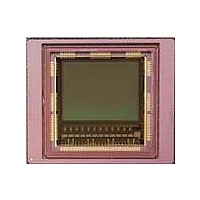
IMAGE SENSOR CMOS LUPA-1300-3
Manufacturer
Cypress Semiconductor Corp
Type
CMOS Imagingr
Specifications of CYIL2SM1300AA-GZDC
Package / Case
168-PGA
Pixel Size
14µm x 14µm
Active Pixel Array
1280H x 1024V
Frames Per Second
500
Voltage - Supply
2.5V, 3.3V
Operating Supply Voltage
2.5 V
Maximum Power Dissipation
1350 mW
Maximum Operating Temperature
+ 70 C
Supply Current
80 mA
Minimum Operating Temperature
0 C
Package
168CuPGA
Image Size
1280x1024 Pixels
Color Sensing
Monochrome
Operating Temperature
0 to 70 °C
Lead Free Status / RoHS Status
Lead free / RoHS Compliant
Lead Free Status / RoHS Status
Lead free / RoHS Compliant, Lead free / RoHS Compliant


Y4_end (74 and 75, 10 bit). These registers set the Y end
address for window 4 (if enabled).
X4_kernels (75, 6 bit). This register sets the number of kernels
or X width to be read out for window 4 (if enabled).
Res_length (76 and 77). This register sets the length of the
internal pixel array reset (how long are all pixel reset
simultaneously). This value is expressed in 'number of lines' or
in clock cycles (depends on seqmode3[6]).
Res_dsts_length. This register sets the length of the internal
dual and triple slope reset pulses when enabled. This value is
expressed in 'number of lines' or in clock cycles (depends on
seqmode3[6]).
Tint_timer (79 and 80). This register sets the length of the
integration time. This value is expressed in 'number of lines' or
in clock cycles (depends on seqmode3[6]).
Tint_ds_timer (81 and 82). This register sets the length of the
dual slope integration time. This value is expressed in 'number
of lines' or in clock cycles (depends on seqmode3[6]).
Tint_ts_timer (83 and 84). This register sets the length of the
triple slope integration time. This value is expressed in 'number
of lines' or in clock cycles (depends on seqmode3[6]).
Serial Peripheral Interface (SPI)
The serial 4-wire interface (or SPI) uses a serial input or output
to shift the data in or out the register buffer. The chip's configu-
ration registers are accessed from the outside world through the
SPI protocol. A 4-wire bus runs over the chip and connects the
SPI I/Os with the internal register blocks. To upload the sensor,
follow this sequence:
The 'out' line is held to High Z. The data for the address A is transferred from the shift register to the active register bank (that is,
sampled) on a rising edge of cs_n. Only the register block with address A can write its data on the 'out' bus. The data on 'in' is ignored.
Document Number: 001-24599 Rev. *F
Figure 10. Read Access (C='0')
Figure 9. Write Access (C='1')
Disable Sequencer → Upload Sensor for new setting → Enable
Sequencer
When sequencer is disabled, the training pattern appears on all
the channels, including the sync. The interface consists of:
■
■
■
■
SPI Protocol
The information on the data 'in' line is:
■
■
■
The data 'out' line is generally in High Z mode, except when a
read request is performed.
Data is always written on the bus on the falling edge of the clock,
and sampled on the rising edge, as seen in
Figure
clock must be active to keep the SPI uploads stored on the chip.
The SPI clock speed must be slower by a factor of 30 when
compared to the system clock (315 MHz nominal speed).
cs_n: chip select, when LOW the chip is selected
clk: the spi clock
in: Master out, Slave in, the serial input of the register
out: Master in, Slave out, the serial output of the register
A command bit C, indicating a write ('1') or a read ('0') access
7-bit address
8-bit data word (in case of a write access)
10. This is valid for both the 'in' and 'out' bus. The system
CYIL2SM1300AA
Page 17 of 43
Figure 9
and
[+] Feedback
Related parts for CYIL2SM1300AA-GZDC
Image
Part Number
Description
Manufacturer
Datasheet
Request
R

Part Number:
Description:
BOARD EVAL IMG SENS LUPA-1300-2
Manufacturer:
Cypress Semiconductor Corp
Datasheet:
Part Number:
Description:
Manufacturer:
Cypress Semiconductor Corp
Datasheet:
Part Number:
Description:
Manufacturer:
Cypress Semiconductor Corp
Datasheet:
Part Number:
Description:
Manufacturer:
Cypress Semiconductor Corp
Datasheet:
Part Number:
Description:
Manufacturer:
Cypress Semiconductor Corp
Datasheet:
Part Number:
Description:
Manufacturer:
Cypress Semiconductor Corp
Datasheet: