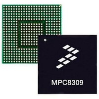
MPC8309VMAHFCA Freescale Semiconductor, MPC8309VMAHFCA Datasheet - Page 12

MPC8309VMAHFCA
Manufacturer Part Number
MPC8309VMAHFCA
Description
417/333/233 MP Std Tmp
Manufacturer
Freescale Semiconductor
Datasheet
1.MPC8309VMAHFCA.pdf
(81 pages)
Specifications of MPC8309VMAHFCA
Processor Series
MPC8309
Core
e300c3
Data Bus Width
32 bit
Data Ram Size
512 MB
Interface Type
USB, CAN, UART, PCI
Maximum Clock Frequency
417 MHz
Number Of Programmable I/os
56
Operating Supply Voltage
- 0.3 V to + 1.26 V
Maximum Operating Temperature
+ 105 C
Mounting Style
SMD/SMT
Operating Temperature Range
0 C to + 105 C
Processor To Be Evaluated
MPC8309
Supply Current (max)
5 uA
Lead Free Status / Rohs Status
Details
Available stocks
Company
Part Number
Manufacturer
Quantity
Price
Company:
Part Number:
MPC8309VMAHFCA
Manufacturer:
Freescale Semiconductor
Quantity:
10 000
Clock Input Timing
The following table shows the estimated typical I/O power dissipation for the device.
4
This section provides the clock input DC and AC electrical characteristics for the MPC8309.
4.1
The following table provides the clock input (SYS_CLK_IN/PCI_SYNC_IN) DC specifications for the
MPC8309. These specifications are also applicable for QE_CLK_IN.
12
DDR I/O
65% utilization
1.8 V
R
R
1 pair of clocks
Local bus I/O load = 25 pF
1 pair of clocks
QUICC Engine block and other I/Os
Note:
1. Typical IO power is based on a nominal voltage of V
Input high voltage
Input low voltage
SYS_CLK_IN input current
SYS_CLK_IN input current
SYS_CLK_IN input current
s
t
benchmark application. The measurements were taken on the evaluation board using WC process silicon.
= 50
= 20
MPC8309 PowerQUICC II Pro Integrated Communications Processor Family Hardware Specifications, Rev. 1
Clock Input Timing
DC Electrical Characteristics
Parameter
Interface
The rise/fall time on QUICC Engine input pins should not exceed 5 ns. This
should be enforced especially on clock signals. Rise time refers to signal
transitions from 10% to 90% of OV
90% to 10% of OV
Table 7. SYS_CLK_IN DC Electrical Characteristics
OV
0.5 V V
Table 6. Typical I/O Power Dissipation
DD
DD
0 V V
0 V V
.
– 0.5 V V
266 MHz, 1 16 bits
66 MHz, 26 bits
TDM serial, HDLC/TRAN serial,
DUART, MII, RMII, Ethernet
management, USB, PCI, SPI, Timer
output, FlexCAN, eSDHC
Condition
IN
IN
OV
IN
—
—
0.5 V or
OV
DD
DD
IN
= 3.3V, ambient temperature, and the core running a Dhrystone
DD
OV
– 0.5 V
Parameter
NOTE
DD
DD
; fall time refers to transitions from
Symbol
V
V
I
I
I
IN
IN
IN
IH
IL
(1.8 V)
GV
0.149
—
–0.3
Min
2.4
DD
—
—
—
(3.3 V)
OV
0.415
—
DD
Freescale Semiconductor
OV
DD
Max
±50
0.4
Unit
±5
±5
W
W
+ 0.3
Comments
—
Unit
1
A
A
A
V
V


