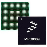
MPC8309VMAHFCA Freescale Semiconductor, MPC8309VMAHFCA Datasheet - Page 76

MPC8309VMAHFCA
Manufacturer Part Number
MPC8309VMAHFCA
Description
417/333/233 MP Std Tmp
Manufacturer
Freescale Semiconductor
Datasheet
1.MPC8309VMAHFCA.pdf
(81 pages)
Specifications of MPC8309VMAHFCA
Processor Series
MPC8309
Core
e300c3
Data Bus Width
32 bit
Data Ram Size
512 MB
Interface Type
USB, CAN, UART, PCI
Maximum Clock Frequency
417 MHz
Number Of Programmable I/os
56
Operating Supply Voltage
- 0.3 V to + 1.26 V
Maximum Operating Temperature
+ 105 C
Mounting Style
SMD/SMT
Operating Temperature Range
0 C to + 105 C
Processor To Be Evaluated
MPC8309
Supply Current (max)
5 uA
Lead Free Status / Rohs Status
Details
Available stocks
Company
Part Number
Manufacturer
Quantity
Price
Company:
Part Number:
MPC8309VMAHFCA
Manufacturer:
Freescale Semiconductor
Quantity:
10 000
System Design Information
25.2
Each of the PLLs listed above is provided with power through independent power supply pins. The voltage
level at each AV
directly from V
There are a number of ways to reliably provide power to the PLLs, but the recommended solution is to
provide independent filter circuits as illustrated in
providing independent filters to each PLL the opportunity to cause noise injection from one PLL to the
other is reduced.
This circuit is intended to filter noise in the PLLs resonant frequency range from a 500 kHz to 10 MHz
range. It should be built with surface mount capacitors with minimum effective series inductance (ESL).
Consistent with the recommendations of Dr. Howard Johnson in High Speed Digital Design: A Handbook
of Black Magic (Prentice Hall, 1993), multiple small capacitors of equal value are recommended over a
single large value capacitor.
Each circuit should be placed as close as possible to the specific AV
noise coupled from nearby circuits. It should be possible to route directly from the capacitors to the AV
pin, which is on the periphery of package, without the inductance of vias.
The following figure shows the PLL power supply filter circuit.
25.3
Due to large address and data buses, and high operating frequencies, the MPC8309 can generate transient
power surges and high frequency noise in its power supply, especially while driving large capacitive loads.
This noise must be prevented from reaching other components in the MPC8309 system, and MPC8309
itself requires a clean, tightly regulated source of power. Therefore, it is recommended that the system
designer place at least one decoupling capacitor at each V
These decoupling capacitors should receive their power from separate V
power planes in the PCB, utilizing short traces to minimize inductance. Capacitors may be placed directly
under the device using a standard escape pattern. Others may surround the part.
These capacitors should have a value of 0.01 or 0.1 µF. Only ceramic SMT (surface mount technology)
capacitors should be used to minimize lead inductance, preferably 0402 or 0603 sizes.
In addition, it is recommended that there be several bulk storage capacitors distributed around the PCB,
feeding the V
These bulk capacitors should have a low ESR (equivalent series resistance) rating to ensure the quick
response time necessary. They should also be connected to the power and ground planes through two vias
76
MPC8309 PowerQUICC II Pro Integrated Communications Processor Family Hardware Specifications, Rev. 1
PLL Power Supply Filtering
Decoupling Recommendations
DD
DD
DD
, OV
V
DD
through a low frequency filter scheme such as the following.
n pin should always be equivalent to V
DD
, and GV
10
Figure 46. PLL Power Supply Filter Circuit
DD
planes, to enable quick recharging of the smaller chip capacitors.
2.2 µF
GND
Figure
Low ESL Surface Mount Capacitors (<0.5 nH)
2.2 µF
46, one to each of the three AV
DD
DD
, OV
, and preferably these voltages are derived
AV
DD
DD
DD
, and GV
pin being supplied to minimize
DD
, OV
DD
DD
pins of the MPC8309.
, GV
Freescale Semiconductor
DD
DD
, and GND
pins. By
DD


