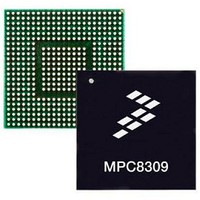
MPC8309VMAHFCA Freescale Semiconductor, MPC8309VMAHFCA Datasheet - Page 40

MPC8309VMAHFCA
Manufacturer Part Number
MPC8309VMAHFCA
Description
417/333/233 MP Std Tmp
Manufacturer
Freescale Semiconductor
Datasheet
1.MPC8309VMAHFCA.pdf
(81 pages)
Specifications of MPC8309VMAHFCA
Processor Series
MPC8309
Core
e300c3
Data Bus Width
32 bit
Data Ram Size
512 MB
Interface Type
USB, CAN, UART, PCI
Maximum Clock Frequency
417 MHz
Number Of Programmable I/os
56
Operating Supply Voltage
- 0.3 V to + 1.26 V
Maximum Operating Temperature
+ 105 C
Mounting Style
SMD/SMT
Operating Temperature Range
0 C to + 105 C
Processor To Be Evaluated
MPC8309
Supply Current (max)
5 uA
Lead Free Status / Rohs Status
Details
Available stocks
Company
Part Number
Manufacturer
Quantity
Price
Company:
Part Number:
MPC8309VMAHFCA
Manufacturer:
Freescale Semiconductor
Quantity:
10 000
eSDHC
The following figure provides the eSDHC clock input timing diagram.
The following figure provides the data and command input/output timing diagram.
40
At recommended operating conditions with OV
Input hold times: SD_CMD, SD_DATx, SD_CD to
SD_CLK
Output delay time: SD_CLK to SD_CMD, SD_DATx valid
Notes:
1. The symbols used for timing specifications herein follow the pattern of t
2. In full-speed mode, the clock frequency value can be 0–25 MHz for an SD/SDIO card and 0–20 MHz for an MMC card. In
3. To satisfy hold timing, the delay difference between clock input and cmd/data input must not exceed 2 ns.
4. C
(reference)(state)
symbolizes eSDHC high-speed mode device timing (SHS) clock reference (K) going to the high (H) state, with respect to the
output (O) reaching the invalid state (X) or output hold time. Note that in general, the clock reference symbol is based on five
letters representing the clock of a particular functional. For rise and fall times, the latter convention is used with the
appropriate letter: R (rise) or F (fall).
high-speed mode, the clock frequency value can be 0–33.25 MHz for an SD/SDIO card and 0–52 MHz for an MMC card.
CARD
MPC8309 PowerQUICC II Pro Integrated Communications Processor Family Hardware Specifications, Rev. 1
Figure 31. eSDHC Data and Command Input/Output Timing Diagram Referenced to Clock
10 pF, (1 card), and C
External Clock
operational mode
SD_DAT/CMD
SD_DAT/CMD
External Clock
for inputs and t
SD_CK
Outputs
eSDHC
Parameter
Inputs
Table 40. eSDHC AC Timing Specifications (continued)
VM
(first three letters of functional block)(reference)(state)(signal)(state)
L
= C
Figure 30. eSDHC Clock Input Timing Diagram
BUS
VM
DD
+ C
= 3.3 V
HOST
VM = Midpoint Voltage (OV
VM = Midpoint Voltage (OV
t
SHSCK
+ C
t
VM
SHSKHOV
t
CARD
VM
SHSIVKH
40 pF
t
Symbol
t
SHSKHOV
SHSIXKH
VM
VM
1
(first three letters of functional block)(signal)(state)
DD
DD
/2)
/2)
t
SHSIXKH
Min
t
2.5
–3
SHSCKL
t
SHSCKR
for outputs. For example, t
VM
t
Max
SHSCKH
—
3
t
SHSCKF
Freescale Semiconductor
Unit
ns
ns
FHSKHOV
Notes
3, 4
4


