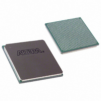
EP2SGX30DF780C5N Altera, EP2SGX30DF780C5N Datasheet - Page 304

EP2SGX30DF780C5N
Manufacturer Part Number
EP2SGX30DF780C5N
Description
IC STRATIX II GX 30K 780-FBGA
Manufacturer
Altera
Series
Stratix® II GXr
Datasheet
1.EP2SGX30DF780C5.pdf
(316 pages)
Specifications of EP2SGX30DF780C5N
Number Of Logic Elements/cells
33880
Number Of Labs/clbs
1694
Total Ram Bits
1369728
Number Of I /o
361
Voltage - Supply
1.15 V ~ 1.25 V
Mounting Type
Surface Mount
Operating Temperature
0°C ~ 70°C
Package / Case
780-FBGA
Family Name
Stratix II GX
Number Of Logic Blocks/elements
33880
# I/os (max)
361
Frequency (max)
609.76MHz
Process Technology
SRAM
Operating Supply Voltage (typ)
1.2V
Logic Cells
33880
Ram Bits
1369728
Operating Supply Voltage (min)
1.15V
Operating Supply Voltage (max)
1.25V
Operating Temp Range
0C to 85C
Operating Temperature Classification
Commercial
Mounting
Surface Mount
Pin Count
780
Package Type
FC-FBGA
Lead Free Status / RoHS Status
Lead free / RoHS Compliant
Number Of Gates
-
Lead Free Status / Rohs Status
Compliant
Other names
544-1754
Available stocks
Company
Part Number
Manufacturer
Quantity
Price
Part Number:
EP2SGX30DF780C5N
Manufacturer:
ALTERA/阿尔特拉
Quantity:
20 000
- Current page: 304 of 316
- Download datasheet (2Mb)
JTAG Timing
Specifications
Figure 4–14
(1)
(1)
(2)
(3)
Table 4–115. DQS Bus Clock Skew Adder Specifications
(t
Table 4–116. DQS Phase Offset Delay Per Stage (ps)
DQS
This skew specification is the absolute maximum and minimum skew. For
example, skew on a 40 DQ group is 40 ps or 20 ps.
The delay settings are linear.
The valid settings for phase offset are -32 to +31.
The typical value equals the average of the minimum and maximum values.
Speed Grade
_CLOCK_SKEW_ADDER)
-3
-4
-5
18 DQ per DQS
36 DQ per DQS
4 DQ per DQS
9 DQ per DQS
shows the timing requirements for the JTAG signals
Mode
Min
Positive Offset
10
10
10
Max
15
15
16
DQS Clock Skew Adder (ps)
Min
Negative Offset
Notes
8
8
8
40
70
75
95
(1), (2),
Max
11
11
12
(1)
(3)
Related parts for EP2SGX30DF780C5N
Image
Part Number
Description
Manufacturer
Datasheet
Request
R

Part Number:
Description:
CYCLONE II STARTER KIT EP2C20N
Manufacturer:
Altera
Datasheet:

Part Number:
Description:
CPLD, EP610 Family, ECMOS Process, 300 Gates, 16 Macro Cells, 16 Reg., 16 User I/Os, 5V Supply, 35 Speed Grade, 24DIP
Manufacturer:
Altera Corporation
Datasheet:

Part Number:
Description:
CPLD, EP610 Family, ECMOS Process, 300 Gates, 16 Macro Cells, 16 Reg., 16 User I/Os, 5V Supply, 15 Speed Grade, 24DIP
Manufacturer:
Altera Corporation
Datasheet:

Part Number:
Description:
Manufacturer:
Altera Corporation
Datasheet:

Part Number:
Description:
CPLD, EP610 Family, ECMOS Process, 300 Gates, 16 Macro Cells, 16 Reg., 16 User I/Os, 5V Supply, 30 Speed Grade, 24DIP
Manufacturer:
Altera Corporation
Datasheet:

Part Number:
Description:
High-performance, low-power erasable programmable logic devices with 8 macrocells, 10ns
Manufacturer:
Altera Corporation
Datasheet:

Part Number:
Description:
High-performance, low-power erasable programmable logic devices with 8 macrocells, 7ns
Manufacturer:
Altera Corporation
Datasheet:

Part Number:
Description:
Classic EPLD
Manufacturer:
Altera Corporation
Datasheet:

Part Number:
Description:
High-performance, low-power erasable programmable logic devices with 8 macrocells, 10ns
Manufacturer:
Altera Corporation
Datasheet:

Part Number:
Description:
Manufacturer:
Altera Corporation
Datasheet:

Part Number:
Description:
Manufacturer:
Altera Corporation
Datasheet:

Part Number:
Description:
Manufacturer:
Altera Corporation
Datasheet:

Part Number:
Description:
CPLD, EP610 Family, ECMOS Process, 300 Gates, 16 Macro Cells, 16 Reg., 16 User I/Os, 5V Supply, 25 Speed Grade, 24DIP
Manufacturer:
Altera Corporation
Datasheet:


