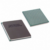
EP2SGX30DF780C5N Altera, EP2SGX30DF780C5N Datasheet - Page 37

EP2SGX30DF780C5N
Manufacturer Part Number
EP2SGX30DF780C5N
Description
IC STRATIX II GX 30K 780-FBGA
Manufacturer
Altera
Series
Stratix® II GXr
Datasheet
1.EP2SGX30DF780C5.pdf
(316 pages)
Specifications of EP2SGX30DF780C5N
Number Of Logic Elements/cells
33880
Number Of Labs/clbs
1694
Total Ram Bits
1369728
Number Of I /o
361
Voltage - Supply
1.15 V ~ 1.25 V
Mounting Type
Surface Mount
Operating Temperature
0°C ~ 70°C
Package / Case
780-FBGA
Family Name
Stratix II GX
Number Of Logic Blocks/elements
33880
# I/os (max)
361
Frequency (max)
609.76MHz
Process Technology
SRAM
Operating Supply Voltage (typ)
1.2V
Logic Cells
33880
Ram Bits
1369728
Operating Supply Voltage (min)
1.15V
Operating Supply Voltage (max)
1.25V
Operating Temp Range
0C to 85C
Operating Temperature Classification
Commercial
Mounting
Surface Mount
Pin Count
780
Package Type
FC-FBGA
Lead Free Status / RoHS Status
Lead free / RoHS Compliant
Number Of Gates
-
Lead Free Status / Rohs Status
Compliant
Other names
544-1754
Available stocks
Company
Part Number
Manufacturer
Quantity
Price
Part Number:
EP2SGX30DF780C5N
Manufacturer:
ALTERA/阿尔特拉
Quantity:
20 000
- Current page: 37 of 316
- Download datasheet (2Mb)
Altera Corporation
October 2007
reduce the interface speed. For example, at 6.375 Gbps, the transceiver
logic has a double-byte-wide data path that runs at 318.75 MHz in a ×20
deserializer factor, which is above the maximum FPGA interface speed.
When using the byte deserializer, the FPGA interface width doubles to
40-bits (36-bits when using the 8B/10B encoder) and the interface speed
reduces to 159.375 MHz.
Byte Ordering Block
The byte ordering block shifts the byte order. A pre-programmed byte in
the input data stream is detected and placed in the least significant byte
of the output stream. Subsequent bytes start appearing in the byte
positions following the LSB. The byte ordering block inserts the
programmed PAD characters to shift the byte order pattern to the LSB.
Based on the setting in the MegaWizard
ordering block can be enabled either by the rx_syncstatus signal or by
the rx_enabyteord signal from the PLD. When the rx_syncstatus
signal is used as enable, the byte ordering block reorders the data only for
the first occurrence of the byte order pattern that is received after word
alignment is completed. You must assert rx_digitalreset to perform
byte ordering again. However, when the byte ordering block is controlled
by rx_enabyteord, the byte ordering block can be controlled by the
PLD logic dynamically. When you create your functional mode in the
MegaWizard, you can select byte ordering block only if rate matcher is
not selected.
Receiver Phase Compensation FIFO Buffer
The receiver phase compensation FIFO buffer resides in the transceiver
block at the FPGA boundary and cannot be bypassed. This FIFO buffer
compensates for phase differences and clock tree timing skew between
the receiver clock domain within the transceiver and the receiver FPGA
clock after it has transferred to the FPGA.
Table 2–9. Byte Deserializer Input and Output Widths
Input Data Width (Bits)
20
16
10
8
Stratix II GX Device Handbook, Volume 1
Deserialized Output Data Width to the
®
Plug-In Manager, the byte
Stratix II GX Architecture
FPGA (Bits)
40
32
20
16
2–29
Related parts for EP2SGX30DF780C5N
Image
Part Number
Description
Manufacturer
Datasheet
Request
R

Part Number:
Description:
CYCLONE II STARTER KIT EP2C20N
Manufacturer:
Altera
Datasheet:

Part Number:
Description:
CPLD, EP610 Family, ECMOS Process, 300 Gates, 16 Macro Cells, 16 Reg., 16 User I/Os, 5V Supply, 35 Speed Grade, 24DIP
Manufacturer:
Altera Corporation
Datasheet:

Part Number:
Description:
CPLD, EP610 Family, ECMOS Process, 300 Gates, 16 Macro Cells, 16 Reg., 16 User I/Os, 5V Supply, 15 Speed Grade, 24DIP
Manufacturer:
Altera Corporation
Datasheet:

Part Number:
Description:
Manufacturer:
Altera Corporation
Datasheet:

Part Number:
Description:
CPLD, EP610 Family, ECMOS Process, 300 Gates, 16 Macro Cells, 16 Reg., 16 User I/Os, 5V Supply, 30 Speed Grade, 24DIP
Manufacturer:
Altera Corporation
Datasheet:

Part Number:
Description:
High-performance, low-power erasable programmable logic devices with 8 macrocells, 10ns
Manufacturer:
Altera Corporation
Datasheet:

Part Number:
Description:
High-performance, low-power erasable programmable logic devices with 8 macrocells, 7ns
Manufacturer:
Altera Corporation
Datasheet:

Part Number:
Description:
Classic EPLD
Manufacturer:
Altera Corporation
Datasheet:

Part Number:
Description:
High-performance, low-power erasable programmable logic devices with 8 macrocells, 10ns
Manufacturer:
Altera Corporation
Datasheet:

Part Number:
Description:
Manufacturer:
Altera Corporation
Datasheet:

Part Number:
Description:
Manufacturer:
Altera Corporation
Datasheet:

Part Number:
Description:
Manufacturer:
Altera Corporation
Datasheet:

Part Number:
Description:
CPLD, EP610 Family, ECMOS Process, 300 Gates, 16 Macro Cells, 16 Reg., 16 User I/Os, 5V Supply, 25 Speed Grade, 24DIP
Manufacturer:
Altera Corporation
Datasheet:


