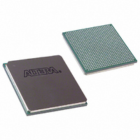
EP2SGX30DF780C5N Altera, EP2SGX30DF780C5N Datasheet - Page 310

EP2SGX30DF780C5N
Manufacturer Part Number
EP2SGX30DF780C5N
Description
IC STRATIX II GX 30K 780-FBGA
Manufacturer
Altera
Series
Stratix® II GXr
Datasheet
1.EP2SGX30DF780C5.pdf
(316 pages)
Specifications of EP2SGX30DF780C5N
Number Of Logic Elements/cells
33880
Number Of Labs/clbs
1694
Total Ram Bits
1369728
Number Of I /o
361
Voltage - Supply
1.15 V ~ 1.25 V
Mounting Type
Surface Mount
Operating Temperature
0°C ~ 70°C
Package / Case
780-FBGA
Family Name
Stratix II GX
Number Of Logic Blocks/elements
33880
# I/os (max)
361
Frequency (max)
609.76MHz
Process Technology
SRAM
Operating Supply Voltage (typ)
1.2V
Logic Cells
33880
Ram Bits
1369728
Operating Supply Voltage (min)
1.15V
Operating Supply Voltage (max)
1.25V
Operating Temp Range
0C to 85C
Operating Temperature Classification
Commercial
Mounting
Surface Mount
Pin Count
780
Package Type
FC-FBGA
Lead Free Status / RoHS Status
Lead free / RoHS Compliant
Number Of Gates
-
Lead Free Status / Rohs Status
Compliant
Other names
544-1754
Available stocks
Company
Part Number
Manufacturer
Quantity
Price
Part Number:
EP2SGX30DF780C5N
Manufacturer:
ALTERA/阿尔特拉
Quantity:
20 000
- Current page: 310 of 316
- Download datasheet (2Mb)
June 2006, v4.0
Table 4–118. Document Revision History (Part 4 of 5)
Document
Date and
Version
●
●
●
●
●
●
●
●
●
●
●
●
●
●
●
●
●
●
Updated Table 6–5.
Updated Table 6–6.
Updated all values in Table 6–7.
Added Tables 6–8 and 6–9.
Added Figures 6–1 through 6–4.
Updated Table 6–18.
Updated Tables 6–85 through 6–96.
Added Table 6–80, Stratix II GX Maximum
Output Clock Rate for Dedicated Clock Pins.
Updated Table 6–100.
In “I/O Timing Measurement Methodology”
section, updated Table 6–42.
In “Internal Timing Parameters” section,
updated Tables 6–43 through 6–48.
In “Stratix II GX Clock Timing Parameters”
section, updated Tables 6–50 through 6–65.
In “IOE Programmable Delay” section, updated
Tables 6–67 and 6–68.
In “I/O Delays” section, updated Tables 6–71
through 6–74.
In “Maximum Input & Output Clock Toggle Rate”
section, updated Tables 6–75 through 6–83.
In “DCD Measurement Techniques” section,
updated Tables 6–85 through 6–92.
In “High-Speed I/O Specifications” section,
updated Tables 6–94 through 6–96.
In “External Memory Interface Specifications”
section, updated Table 6–100.
Changes Made
●
●
●
●
Removed rows for V
and V
Updated values for rx, tx, and
refclkb
Removed table containing 1.2-V
PCML I/O information. That
information is in Table 6–7.
Added values to Table 6–100.
Summary of Changes
O C M
in Table 6–6.
from Table 6–5.
I D
, V
O D
, V
I C M
,
Related parts for EP2SGX30DF780C5N
Image
Part Number
Description
Manufacturer
Datasheet
Request
R

Part Number:
Description:
CYCLONE II STARTER KIT EP2C20N
Manufacturer:
Altera
Datasheet:

Part Number:
Description:
CPLD, EP610 Family, ECMOS Process, 300 Gates, 16 Macro Cells, 16 Reg., 16 User I/Os, 5V Supply, 35 Speed Grade, 24DIP
Manufacturer:
Altera Corporation
Datasheet:

Part Number:
Description:
CPLD, EP610 Family, ECMOS Process, 300 Gates, 16 Macro Cells, 16 Reg., 16 User I/Os, 5V Supply, 15 Speed Grade, 24DIP
Manufacturer:
Altera Corporation
Datasheet:

Part Number:
Description:
Manufacturer:
Altera Corporation
Datasheet:

Part Number:
Description:
CPLD, EP610 Family, ECMOS Process, 300 Gates, 16 Macro Cells, 16 Reg., 16 User I/Os, 5V Supply, 30 Speed Grade, 24DIP
Manufacturer:
Altera Corporation
Datasheet:

Part Number:
Description:
High-performance, low-power erasable programmable logic devices with 8 macrocells, 10ns
Manufacturer:
Altera Corporation
Datasheet:

Part Number:
Description:
High-performance, low-power erasable programmable logic devices with 8 macrocells, 7ns
Manufacturer:
Altera Corporation
Datasheet:

Part Number:
Description:
Classic EPLD
Manufacturer:
Altera Corporation
Datasheet:

Part Number:
Description:
High-performance, low-power erasable programmable logic devices with 8 macrocells, 10ns
Manufacturer:
Altera Corporation
Datasheet:

Part Number:
Description:
Manufacturer:
Altera Corporation
Datasheet:

Part Number:
Description:
Manufacturer:
Altera Corporation
Datasheet:

Part Number:
Description:
Manufacturer:
Altera Corporation
Datasheet:

Part Number:
Description:
CPLD, EP610 Family, ECMOS Process, 300 Gates, 16 Macro Cells, 16 Reg., 16 User I/Os, 5V Supply, 25 Speed Grade, 24DIP
Manufacturer:
Altera Corporation
Datasheet:


