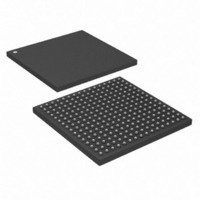
DS26518GN+ Maxim Integrated Products, DS26518GN+ Datasheet - Page 210

DS26518GN+
Manufacturer Part Number
DS26518GN+
Description
IC TXRX T1/E1/J1 8PORT 256-CSBGA
Manufacturer
Maxim Integrated Products
Type
Transceiverr
Specifications of DS26518GN+
Number Of Drivers/receivers
8/8
Protocol
T1/E1/J1
Voltage - Supply
3.135 V ~ 3.465 V
Mounting Type
Surface Mount
Package / Case
256-CSBGA
Lead Free Status / RoHS Status
Lead free / RoHS Compliant
- Current page: 210 of 312
- Download datasheet (3Mb)
Register Name:
Register Description:
Register Address:
Bit #
Name
Default
Note: Also used to insert Fs framing pattern in D4 framing mode.
The Transmit FDL Register (T1TFDL) contains the Facility Data Link (FDL) information that is to be inserted on a
byte basis into the outgoing T1 data stream. The LSB is transmitted first. In D4 mode, only the lower six bits are
used.
Bit 7: Transmit FDL Bit 7 (TFDL7). MSB of the Transmit FDL Code.
Bit 6: Transmit FDL Bit 6 (TFDL6)
Bit 5: Transmit FDL Bit 5 (TFDL5)
Bit 4: Transmit FDL Bit 4 (TFDL4)
Bit 3: Transmit FDL Bit 3 (TFDL3)
Bit 2: Transmit FDL Bit 2 (TFDL2)
Bit 1: Transmit FDL Bit 1 (TFDL1)
Bit 0: Transmit FDL Bit 0 (TFDL0). LSB of the Transmit FDL Code.
Register Name:
Register Description:
Register Address:
Bit #
Name
Default
Bit 5: Transmit BOC Bit 5 (TBOC5). MSB of the transmit BOC code.
Bit 4: Transmit BOC Bit 4 (TBOC4)
Bit 3: Transmit BOC Bit 3 (TBOC3)
Bit 2: Transmit BOC Bit 2 (TBOC2)
Bit 1: Transmit BOC Bit 1 (TBOC1)
Bit 0: Transmit BOC Bit 0 (TBOC0). LSB of the transmit BOC code.
TFDL7
—
7
0
7
0
T1TFDL
Transmit FDL Register
162h + (200h x (n - 1)) : where n = 1 to 8
T1TBOC
Transmit BOC Register
163h + (200h x (n - 1)) : where n = 1 to 8
TFDL6
—
6
0
6
0
TBOC5
TFDL5
5
0
5
0
TBOC4
210 of 312
TFDL4
0
0
4
4
TBOC3
TFDL3
3
0
3
0
TBOC2
TFDL2
2
0
2
0
TBOC1
TFDL1
1
0
1
0
TBOC0
TFDL0
0
0
0
0
Related parts for DS26518GN+
Image
Part Number
Description
Manufacturer
Datasheet
Request
R

Part Number:
Description:
8-port T1/e1/j1 Transceiver
Manufacturer:
Maxim Integrated Products, Inc.
Datasheet:

Part Number:
Description:
Ds26518 8-port T1/e1/j1 Transceiver
Manufacturer:
Maxim Integrated Products, Inc.

Part Number:
Description:
power light source LUXEON� Collimator
Manufacturer:
LUMILEDS [Lumileds Lighting Company]
Datasheet:

Part Number:
Description:
MAX7528KCWPMaxim Integrated Products [CMOS Dual 8-Bit Buffered Multiplying DACs]
Manufacturer:
Maxim Integrated Products
Datasheet:

Part Number:
Description:
Single +5V, fully integrated, 1.25Gbps laser diode driver.
Manufacturer:
Maxim Integrated Products
Datasheet:

Part Number:
Description:
Single +5V, fully integrated, 155Mbps laser diode driver.
Manufacturer:
Maxim Integrated Products
Datasheet:

Part Number:
Description:
VRD11/VRD10, K8 Rev F 2/3/4-Phase PWM Controllers with Integrated Dual MOSFET Drivers
Manufacturer:
Maxim Integrated Products
Datasheet:

Part Number:
Description:
Highly Integrated Level 2 SMBus Battery Chargers
Manufacturer:
Maxim Integrated Products
Datasheet:

Part Number:
Description:
Current Monitor and Accumulator with Integrated Sense Resistor; ; Temperature Range: -40°C to +85°C
Manufacturer:
Maxim Integrated Products

Part Number:
Description:
TSSOP 14/A�/RS-485 Transceivers with Integrated 100O/120O Termination Resis
Manufacturer:
Maxim Integrated Products

Part Number:
Description:
TSSOP 14/A�/RS-485 Transceivers with Integrated 100O/120O Termination Resis
Manufacturer:
Maxim Integrated Products

Part Number:
Description:
QFN 16/A�/AC-DC and DC-DC Peak-Current-Mode Converters with Integrated Step
Manufacturer:
Maxim Integrated Products

Part Number:
Description:
TDFN/A/65V, 1A, 600KHZ, SYNCHRONOUS STEP-DOWN REGULATOR WITH INTEGRATED SWI
Manufacturer:
Maxim Integrated Products

Part Number:
Description:
Integrated Temperature Controller f
Manufacturer:
Maxim Integrated Products


