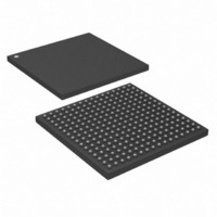
DS26518GN+ Maxim Integrated Products, DS26518GN+ Datasheet - Page 39

DS26518GN+
Manufacturer Part Number
DS26518GN+
Description
IC TXRX T1/E1/J1 8PORT 256-CSBGA
Manufacturer
Maxim Integrated Products
Type
Transceiverr
Specifications of DS26518GN+
Number Of Drivers/receivers
8/8
Protocol
T1/E1/J1
Voltage - Supply
3.135 V ~ 3.465 V
Mounting Type
Surface Mount
Package / Case
256-CSBGA
Lead Free Status / RoHS Status
Lead free / RoHS Compliant
- Current page: 39 of 312
- Download datasheet (3Mb)
9.8.1.7 Mapping E1 Channels onto a 1.544MHz Backplane
The user can use the RSCLKM bit in RIOCR.4 to enable the receive elastic store to operate with a 1.544MHz
backplane (24 channels / frame + F-bit). In this mode the user can choose which of the E1 time slots will be
ignored (not transmitted onto RSERn) by programming the Receive Blank Channel Select registers (RBCS1–4). A
logic 1 in the associated bit location will cause the elastic store to ignore the incoming E1 data for that channel.
Typically, the user will want to program eight channels to be ignored. The default (power-up) configuration will
ignore channels 25 to 32, so that the first 24 E1 channels are mapped into the 24 channels of the 1.544MHz
backplane. In this mode the F-bit location at RSERn is always set to 1.
For example, if the user wants to ignore E1 time slots 0 (channel 1) and TS 16 (channel 17), the RBCS registers
would be programmed as follows:
9.8.2 IBO Multiplexing
The DS26518 offers two methods of multiplexing data streams onto a high-speed backplane bus. The traditional
method of IBO operation that allows the user to gang signals together on the PCB is supported. RSERn and RSIGn
will tri-state at the appropriate times to allow the ganging of these signals together.
The default method multiplexes the data streams internally and then outputs them on one pin, i.e., RSER1. For
example, if the user wants to multiplex RSER[1:8] together to make a 16MHz high-speed bus, the data stream will
be output on RSER1 only.
The selection between external ganging and internal multiplexing is made via GTCR1.GIBO.
Note that in IBO mode, the channel block signals TCHBLKn and RCHBLKn are referenced to as TSYSCLKn and
RSYSCLKn.
Figure
only show channels 1–8.
Table 9-5. Registers Related to the IBO Multiplexer
Note: The addresses shown above are for Framer 1. Addresses for Framers 2 to 8 can be calculated using the following: Framer n = (Framer 1
address + (n - 1) x 200hex), where n = 2 to 8 for Framers 2 to 8.
Global Transceiver Control
Register 1 (GTCR1)
Global Framer Control Register 1
(GFCR1)
Receive Interleave Bus Operation
Control Register (RIBOC)
Transmit Interleave Bus
Operation Control Register
(TIBOC)
9-11,
RBCS1
RBCS2
RBCS3
RBCS4
REGISTER
Figure
= 01h
= 00h
= 01h
= FCh
9-12, and
Table 9-5
Figure 9-13
describes the pin function changes for each mode of the IBO multiplexer.
ADDRESSES
FRAMER 1
00F0h
00F1h
088h
188h
show the equivalent internal circuit for each IBO mode. These figures
39 of 312
This is a global register used to specify ganged operation
for the IBO.
This global register defines the number of devices per
bus and bus speed.
This register configures the per-port IBO enable and type
of interleaving (channel vs. frame).
This register configures the per-port IBO enable and type
of interleaving (channel vs. frame).
FUNCTION
Related parts for DS26518GN+
Image
Part Number
Description
Manufacturer
Datasheet
Request
R

Part Number:
Description:
8-port T1/e1/j1 Transceiver
Manufacturer:
Maxim Integrated Products, Inc.
Datasheet:

Part Number:
Description:
Ds26518 8-port T1/e1/j1 Transceiver
Manufacturer:
Maxim Integrated Products, Inc.

Part Number:
Description:
power light source LUXEON� Collimator
Manufacturer:
LUMILEDS [Lumileds Lighting Company]
Datasheet:

Part Number:
Description:
MAX7528KCWPMaxim Integrated Products [CMOS Dual 8-Bit Buffered Multiplying DACs]
Manufacturer:
Maxim Integrated Products
Datasheet:

Part Number:
Description:
Single +5V, fully integrated, 1.25Gbps laser diode driver.
Manufacturer:
Maxim Integrated Products
Datasheet:

Part Number:
Description:
Single +5V, fully integrated, 155Mbps laser diode driver.
Manufacturer:
Maxim Integrated Products
Datasheet:

Part Number:
Description:
VRD11/VRD10, K8 Rev F 2/3/4-Phase PWM Controllers with Integrated Dual MOSFET Drivers
Manufacturer:
Maxim Integrated Products
Datasheet:

Part Number:
Description:
Highly Integrated Level 2 SMBus Battery Chargers
Manufacturer:
Maxim Integrated Products
Datasheet:

Part Number:
Description:
Current Monitor and Accumulator with Integrated Sense Resistor; ; Temperature Range: -40°C to +85°C
Manufacturer:
Maxim Integrated Products

Part Number:
Description:
TSSOP 14/A�/RS-485 Transceivers with Integrated 100O/120O Termination Resis
Manufacturer:
Maxim Integrated Products

Part Number:
Description:
TSSOP 14/A�/RS-485 Transceivers with Integrated 100O/120O Termination Resis
Manufacturer:
Maxim Integrated Products

Part Number:
Description:
QFN 16/A�/AC-DC and DC-DC Peak-Current-Mode Converters with Integrated Step
Manufacturer:
Maxim Integrated Products

Part Number:
Description:
TDFN/A/65V, 1A, 600KHZ, SYNCHRONOUS STEP-DOWN REGULATOR WITH INTEGRATED SWI
Manufacturer:
Maxim Integrated Products

Part Number:
Description:
Integrated Temperature Controller f
Manufacturer:
Maxim Integrated Products


